RM0453 Rev 5 763/1450
RM0453 Advanced-control timer (TIM1)
821
The two break inputs have different behaviors on timer outputs:
– The BRK input can either disable (inactive state) or force the PWM outputs to a
predefined safe state.
– BRK2 can only disable (inactive state) the PWM outputs.
The BRK has a higher priority than BRK2 input, as described in Table 176.
Note: BRK2 must only be used with OSSR = OSSI = 1.
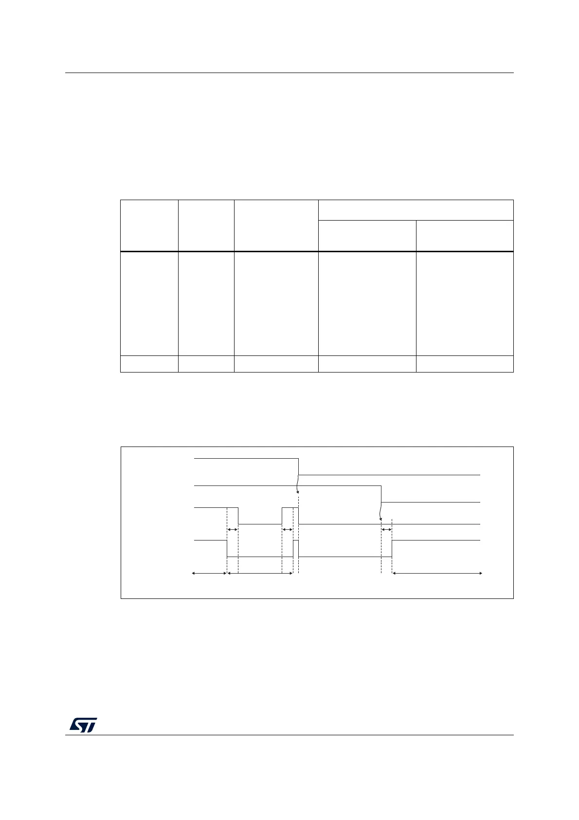
Figure 173 gives an example of OCx and OCxN output behavior in case of active signals on
BRK and BRK2 inputs. In this case, both outputs have active high polarities (CCxP =
CCxNP = 0 in TIMx_CCER register).
Figure 173. PWM output state following BRK and BRK2 pins assertion (OSSI=1)
Table 176. Behavior of timer outputs versus BRK/BRK2 inputs
BRK BRK2
Timer outputs
state
Typical use case
OCxN output
(low side switches)
OCx output
(high side switches)
Active X
– Inactive then
forced output
state (after a
deadtime)
– Outputs disabled
if OSSI = 0
(control taken
over by GPIO
logic)
ON after deadtime
insertion
OFF
Inactive Active Inactive OFF OFF
MS34106V1
BRK2
BRK
OCx
I/O state
Deadtime Deadtime
Active Inactive Idle