General-purpose timer (TIM2) RM0453
862/1450 RM0453 Rev 5
1. Configure TIM1 master mode to send its Output Compare 1 Reference (OC1REF)
signal as trigger output (MMS=100 in the TIM1_CR2 register).
2. Configure the TIM1 OC1REF waveform (TIM1_CCMR1 register).
3. Configure TIM2 to get the input trigger from TIM1 (TS=00000 in the TIM2_SMCR
register).
4. Configure TIM2 in gated mode (SMS=101 in TIM2_SMCR register).
5. Enable TIM2 by writing ‘1 in the CEN bit (TIM_CR1 register).
6. Start TIM by writing ‘1 in the CEN bit (TIM1_CR1 register).
Note: The counter 2 clock is not synchronized with counter 1, this mode only affects the TIM2
counter enable signal.
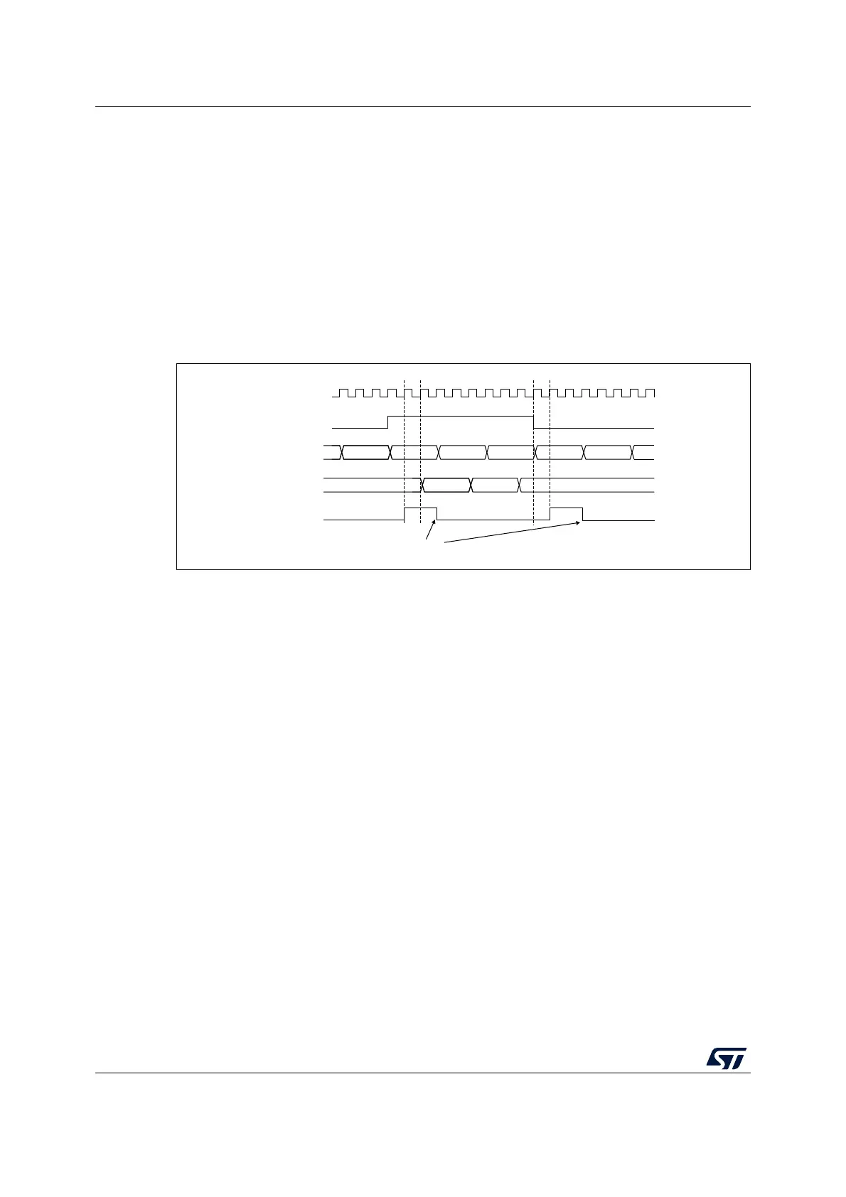
Figure 233. Gating TIM2 with OC1REF of TIM1
In the example in Figure 233, the TIM2 counter and prescaler are not initialized before being
started. So they start counting from their current value. It is possible to start from a given
value by resetting both timers before starting TIM1. Then any value can be written in the
timer counters. The timers can easily be reset by software using the UG bit in the
TIMx_EGR registers.
In the next example (refer to Figure 234), we synchronize TIM1 and TIM2. TIM1 is the
master and starts from 0. TIM2 is the slave and starts from 0xE7. The prescaler ratio is the
same for both timers. TIM2 stops when TIM1 is disabled by writing ‘0 to the CEN bit in the
TIM1_CR1 register:
1. Configure TIM1 master mode to send its Output Compare 1 Reference (OC1REF)
signal as trigger output (MMS=100 in the TIM1_CR2 register).
2. Configure the TIM1 OC1REF waveform (TIM1_CCMR1 register).
3. Configure TIM2 to get the input trigger from TIM1 (TS=00000 in the TIM2_SMCR
register).
4. Configure TIM2 in gated mode (SMS=101 in TIM2_SMCR register).
5. Reset TIM1 by writing ‘1 in UG bit (TIM1_EGR register).
6. Reset TIM2 by writing ‘1 in UG bit (TIM2_EGR register).
7. Initialize TIM2 to 0xE7 by writing ‘0xE7’ in the TIM2 counter (TIM2_CNTL).
8. Enable TIM2 by writing ‘1 in the CEN bit (TIM2_CR1 register).
9. Start TIM1 by writing ‘1 in the CEN bit (TIM1_CR1 register).
10. Stop TIM1 by writing ‘0 in the CEN bit (TIM1_CR1 register).
MS32695V2
CK_INT
FC FD FE FF 00 01
TIM1-OC1REF
TIM1-CNT
30463045 3047 3048
TIM2-CNT
TIM2-TIF
Write TIF = 0