RM0453 Rev 5 539/1450
RM0453 Analog-to-digital converter (ADC)
591
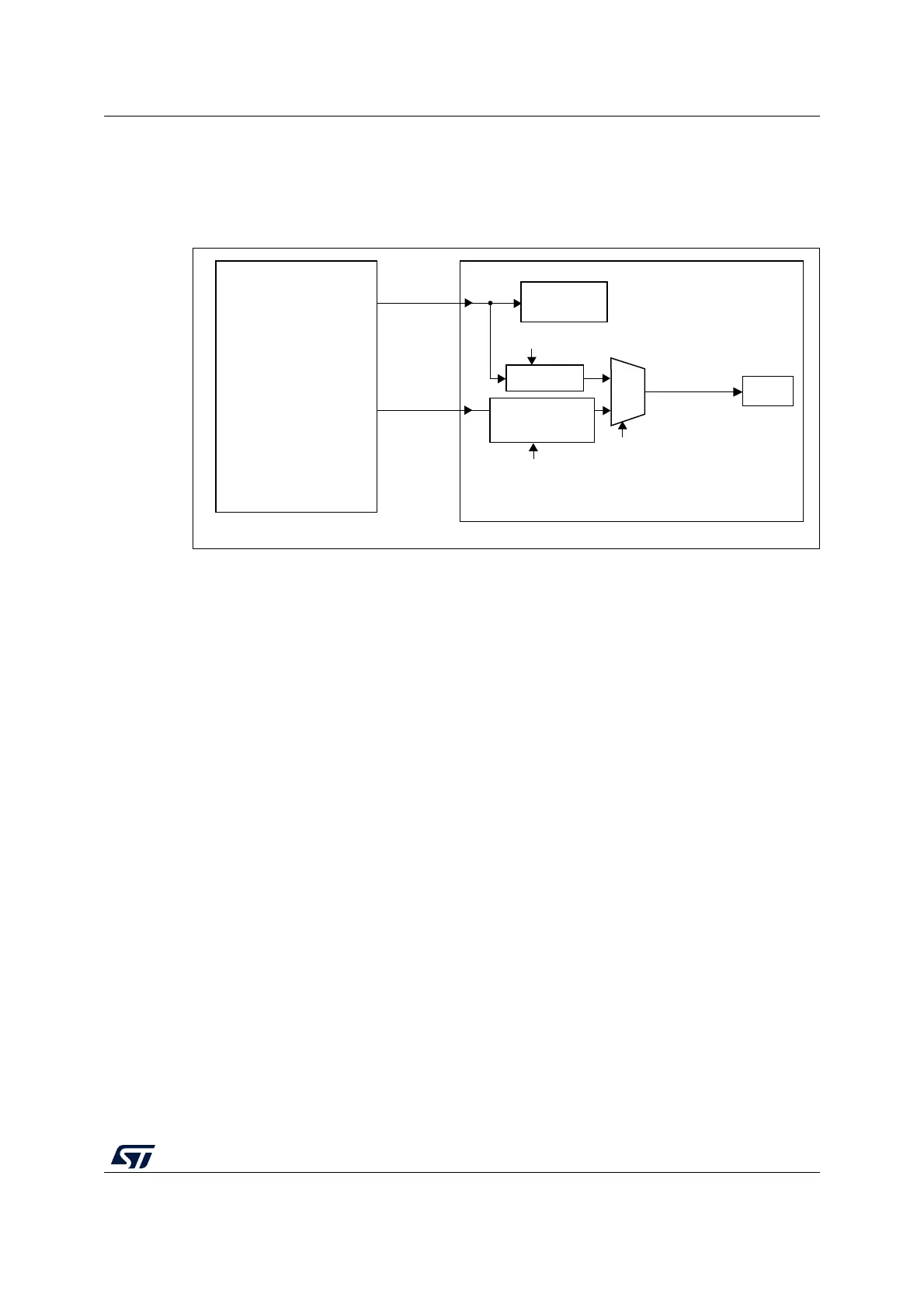
18.3.5 ADC clock (CKMODE, PRESC[3:0])
The ADC has a dual clock-domain architecture, so that the ADC can be fed with a clock
(ADC asynchronous clock) independent from the APB clock (PCLK).
Figure 62. ADC clock scheme
1. Refer to Section Reset and clock control (RCC) for how the PCLK clock and ADC asynchronous clock are
enabled.
The input clock of the analog ADC can be selected between two different clock sources (see
Figure 62: ADC clock scheme to see how the PCLK clock and the ADC asynchronous clock
are enabled):
a) The ADC clock can be a specific clock source, named “ADC asynchronous clock“
which is independent and asynchronous with the APB clock.
Refer to RCC Section for more information on generating this clock source.
To select this scheme, bits CKMODE[1:0] of the ADC_CFGR2 register must be
reset.
b) The ADC clock can be derived from the APB clock of the ADC bus interface,
divided by a programmable factor (1, 2 or 4) according to bits CKMODE[1:0].
To select this scheme, bits CKMODE[1:0] of the ADC_CFGR2 register must be
different from “00”.
In option a), the generated ADC clock can eventually be divided by a prescaler (1, 2, 4, 6, 8,
10, 12, 16, 32, 64, 128, 256) when programming the bits PRESC[3:0] in the ADC_CCR
register).
Option a) has the advantage of reaching the maximum ADC clock frequency whatever the
APB clock scheme selected.
Option b) has the advantage of bypassing the clock domain resynchronizations. This can be
useful when the ADC is triggered by a timer and if the application requires that the ADC is
precisely triggered without any uncertainty (otherwise, an uncertainty of the trigger instant is
added by the resynchronizations between the two clock domains).
MSv31926V2
ADITF
Analog
ADC
RCC
(Reset & Clock Controller)
PCLK
ADC
asynchronous
clock
APB interface
Analog ADC_CK
/1 or /2 or /4
Others
00
Bits CKMODE[1:0]
of ADC_CFGR2
Bits CKMODE[1:0]
of ADC_CFGR2
/1,2,4,6,8,10,12
16,32,64,128,256
Bits PRESC[3:0]
of ADC_CCR