General-purpose I/Os (GPIO) RM0453
406/1450 RM0453 Rev 5
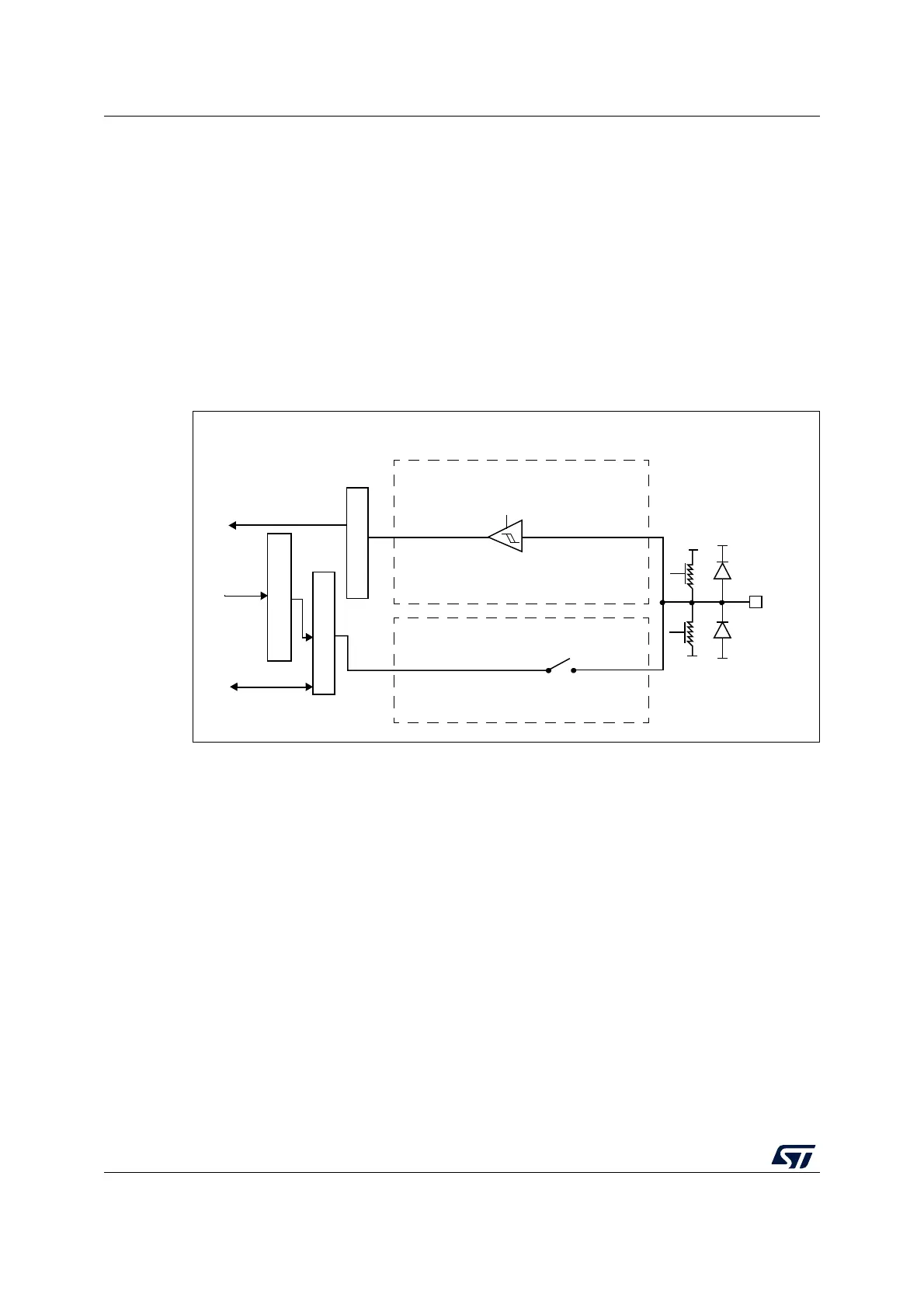
10.3.9 Input configuration
When the I/O port is programmed as input, the following occurs:
• The output buffer is disabled.
• The Schmitt trigger input is activated.
• The pull-up and pull-down resistors are activated depending on the value in the
GPIOx_PUPDR register.
• The data present on the I/O pin are sampled into the input data register every AHB
clock cycle.
• A read access to the input data register provides the I/O state.
The figure below shows the input configuration of the I/O port bit.
Figure 45. Input floating/pull-up/pull-down configurations
10.3.10 Output configuration
When the I/O port is programmed as output, the following occurs:
• The output buffer is enabled:
– Open drain mode: A 0 in the Output register activates the N-MOS whereas a 1 in
the Output register leaves the port in Hi-Z (the P-MOS is never activated).
– Push-pull mode: A 0 in the Output register activates the N-MOS whereas a 1 in the
Output register activates the P-MOS.
• The Schmitt trigger input is activated.
• The pull-up and pull-down resistors are activated depending on the value in the
GPIOx_PUPDR register.
• The data present on the I/O pin are sampled into the input data register every AHB
clock cycle.
• A read access to the input data register gets the I/O state.
• A read access to the output data register gets the last written value.
on/off
pull
pull
on/off
I/O pin
V
DDIOx
V
SS
TTL Schmitt
trigger
V
SS
V
DDIOx
protection
diode
protection
diode
on
input driver
output driver
down
up
Input data register
Output data register
Read/write
Read
Bit set/reset registers
Write
MS31477V1