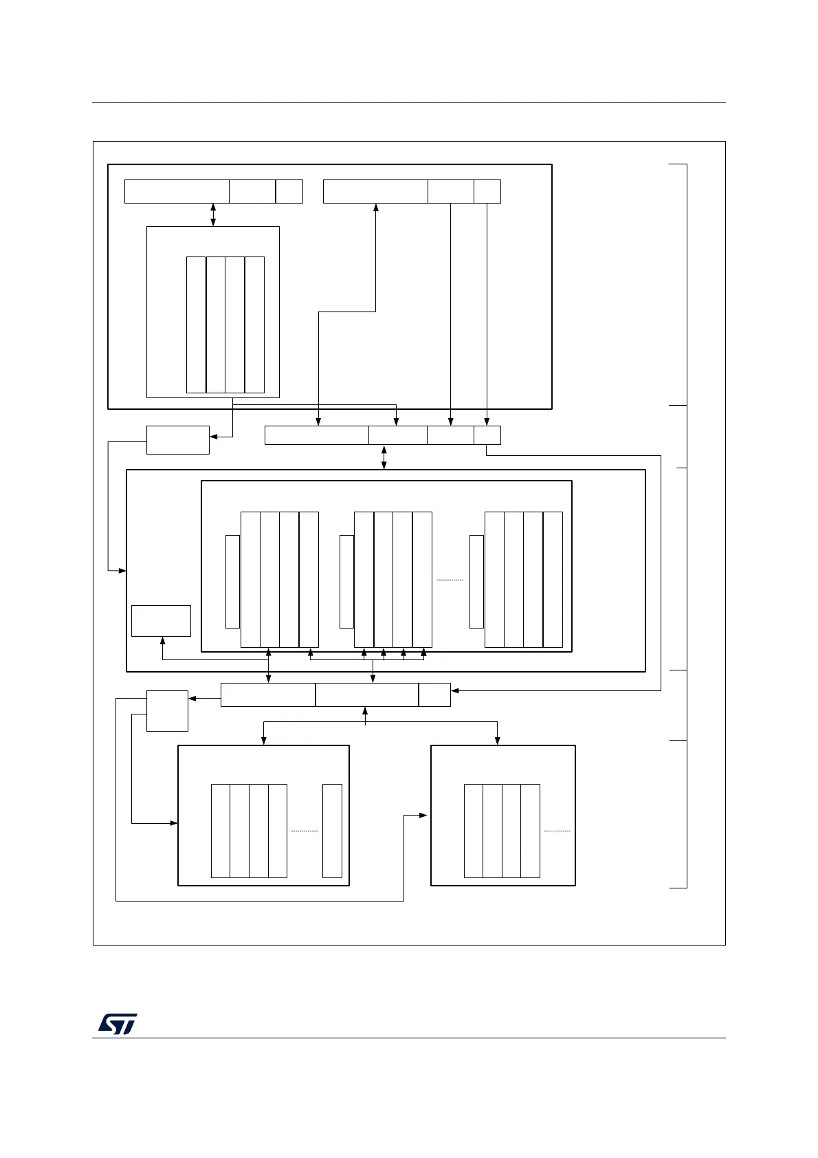
Figure 387. Debugger connection to debug components
MSv60375V1
Register 0
Register 1
Register 2
Register 3
0x000
0x04
0x08
0x0C
0xFFC
Processor
4-Kbyte block
Processor address
Reserved
0x0000 0000
Reserved
0x000
0x004
0x008
0x00C
ROM table
4-Kbyte block
Debug
access
decode
Addr[31:2]
(2)
Data[31:0] RnW
Control/status word (CSW)
Transfer address (TAR)
Reserved
Data read/write (DRW)
Bank 0x0
0x00
0x14
0x18
0x1C
Control/status word (CSW)
Transfer address (TAR)
Reserved
Data read/write (DRW)
Bank 0x1
0x10
0xF4
0xF8
0xFC
Control/status word (CSW)
Transfer address (TAR)
Reserved
Data read/write (DRW)
Bank 0xF
0xF0
Address
incrementer
Memory
access port
(MEM-AP)
APSEL
decode
Data [31:0] A[7:4] A[3:2] RnW
A[7:4] selects the register bank.
A[3:2] selects a register within bank.
(1) This is only a partial view of the DP registers (refer to the DP registers descriptions for more details.
DPACC APACC
Data[31:0] A[3:2] RnW Data[31:0] A[3:2] RnW
0x04
0x08
0x0C
Data link defined
Control/status (CTRLSTAT)
AP select (SELECT)
Read buffer (RDBUFF)
0x00
DP registers
(1)
Debug register files
Resource-specific
transport
Memory access port
AP
access
Debug port
0x004
0x008
0x00C
Register 1023
(2) Register field widths are not to scale. For example, RnW is a single bit.