RM0453 Rev 5 849/1450
RM0453 General-purpose timer (TIM2)
892
26.3.10 Asymmetric PWM mode
Asymmetric mode allows two center-aligned PWM signals to be generated with a
programmable phase shift. While the frequency is determined by the value of the
TIMx_ARR register, the duty cycle and the phase-shift are determined by a pair of
TIMx_CCRx registers. One register controls the PWM during up-counting, the second
during down counting, so that PWM is adjusted every half PWM cycle:
• OC1REFC (or OC2REFC) is controlled by TIMx_CCR1 and TIMx_CCR2
• OC3REFC (or OC4REFC) is controlled by TIMx_CCR3 and TIMx_CCR4
Asymmetric PWM mode can be selected independently on two channels (one OCx output
per pair of CCR registers) by writing ‘1110’ (Asymmetric PWM mode 1) or ‘1111’
(Asymmetric PWM mode 2) in the OCxM bits in the TIMx_CCMRx register.
Note: The OCxM[3:0] bit field is split into two parts for compatibility reasons, the most significant
bit is not contiguous with the 3 least significant ones.
When a given channel is used as asymmetric PWM channel, its secondary channel can also
be used. For instance, if an OC1REFC signal is generated on channel 1 (Asymmetric PWM
mode 1), it is possible to output either the OC2REF signal on channel 2, or an OC2REFC
signal resulting from asymmetric PWM mode 2.
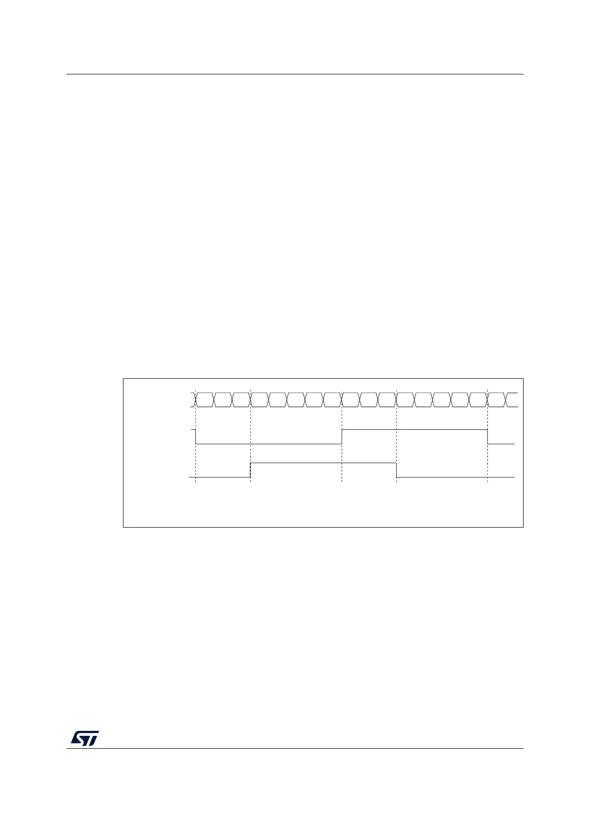
Figure 220 shows an example of signals that can be generated using Asymmetric PWM
mode (channels 1 to 4 are configured in Asymmetric PWM mode 1).
Figure 220. Generation of 2 phase-shifted PWM signals with 50% duty cycle
26.3.11 Combined PWM mode
Combined PWM mode allows two edge or center-aligned PWM signals to be generated with
programmable delay and phase shift between respective pulses. While the frequency is
determined by the value of the TIMx_ARR register, the duty cycle and delay are determined
by the two TIMx_CCRx registers. The resulting signals, OCxREFC, are made of an OR or
AND logical combination of two reference PWMs:
– OC1REFC (or OC2REFC) is controlled by TIMx_CCR1 and TIMx_CCR2
– OC3REFC (or OC4REFC) is controlled by TIMx_CCR3 and TIMx_CCR4
Combined PWM mode can be selected independently on two channels (one OCx output per
pair of CCR registers) by writing ‘1100’ (Combined PWM mode 1) or ‘1101’ (Combined PWM
mode 2) in the OCxM bits in the TIMx_CCMRx register.
MS33117V1
Counter register
OC1REFC
CCR1=0
CCR2=8
CCR3=3
CCR4=5
01234567 012345678 11
OC3REFC