RM0453 Rev 5 593/1450
RM0453 Digital-to-analog converter (DAC)
616
19.3 DAC implementation
19.4 DAC functional description
19.4.1 DAC block diagram
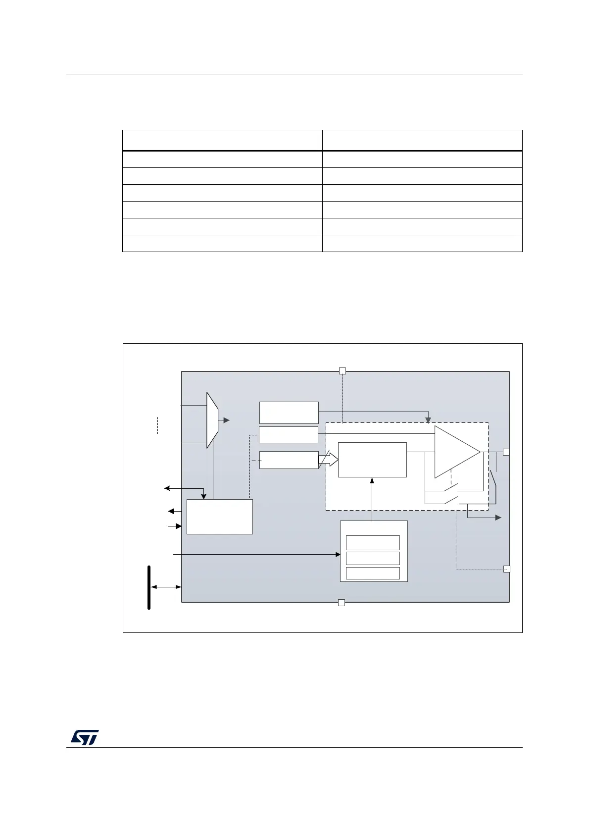
Figure 86. DAC block diagram
1. MODE1 bits in the DAC_MCR control the output mode and allow switching between the Normal mode in
buffer/unbuffered configuration and the Sample and hold mode.
Table 111. DAC features
DAC features DAC
Dual channel -
Output buffer X
I/O connection DAC_OUT1 to PA10
Maximum sampling time 1 Msps
Autonomous mode -
VREF+ pin X
MSv61355V6
V
REF+
dac_out1
DAC_OUT1
Buffer
TSAMPLE1
THOLD1
TREFRESH1
Sample and hold
registers
TSEL1
[3:0]
bits
TRIG
dac_ch1_dma
dac_ch1_trg1
dac_ch1_trg15
32-bit APB
bus
DAC
converter
DOR1
Offset
calibration
OTRIM1[4:0]
bits
12-bit
MODE1 bits
dac_unr_it
dac_pclk
V
DD
V
SS
dac_hold_ck
Control registers
and logic
channel1