RM0453 Rev 5 633/1450
RM0453 True random number generator (RNG)
646
22.3 RNG functional description
22.3.1 RNG block diagram
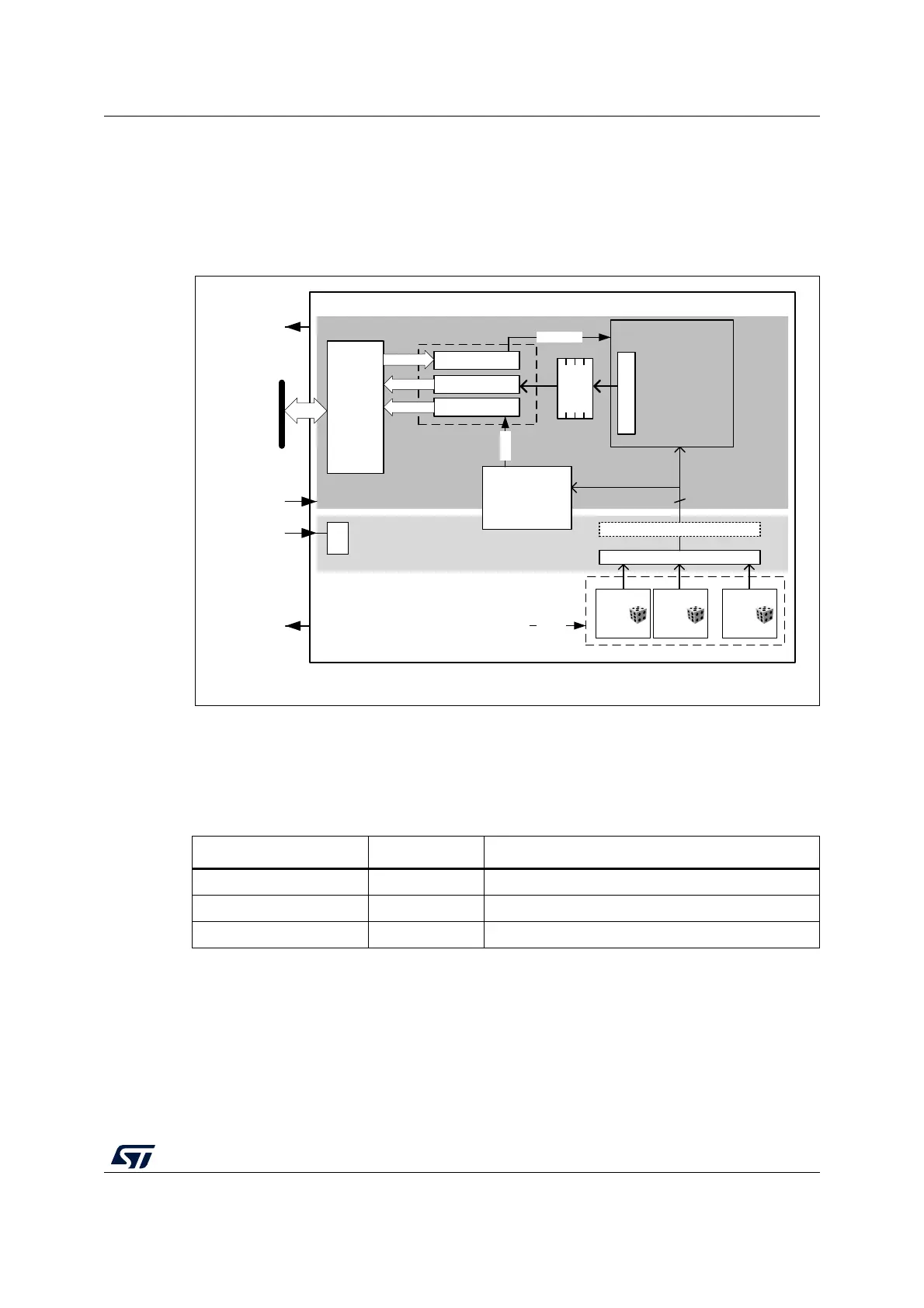
Figure 98 shows the RNG block diagram.
Figure 98. RNG block diagram
22.3.2 RNG internal signals
Table 129 describes a list of useful-to-know internal signals available at the RNG level, not
at the STM32 product level (on pads).
22.3.3 Random number generation
The true random number generator (RNG) delivers truly random data through its AHB
interface at deterministic intervals.
Within its boundary RNG integrates all the required NIST components depicted on
Figure 99. Those components are an analog noise source, a digitization stage, a
MSv42098V3
True RNG
RNG_CR
RNG_SR
AHB
interface
RNG_DR
Analog
noise
source 1
Banked Registers
Sampling (x N) + XOR
DIV
Analog noise source
Fault detection
Clock checker
Health tests
1-bit
CONDRST
Alarms
...
Analog
noise
source 2
Analog
noise
source N
4x32-bit
FIFO
Conditioning logic
128-bit data output
en_osc
rng_it
rng_hclk
rng_clk
AHB clock domain
RNG clock domain
Post-processing (optional)
32-bit AHB bus
rng_itamp_out
Table 129. RNG internal input/output signals
Signal name Signal type Description
rng_it Digital output RNG global interrupt request
rng_hclk Digital input AHB clock
rng_clk Digital input RNG dedicated clock, asynchronous to rng_hclk