AES hardware accelerator (AES) RM0453
680/1450 RM0453 Rev 5
23.4.16 AES DMA interface
The AES peripheral provides an interface to connect to the DMA (direct memory access)
controller. The DMA operation is controlled through the AES_CR register.
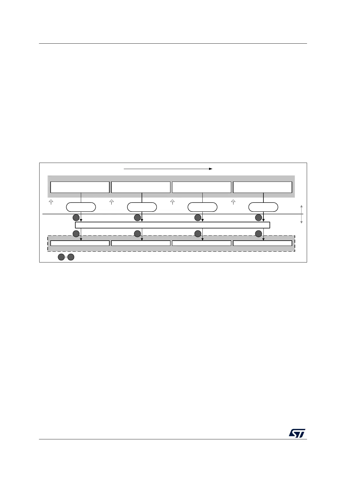
Data input using DMA
Setting the DMAINEN bit of the AES_CR register enables DMA writing into AES. The AES
peripheral then initiates a DMA request during the input phase each time it requires to write
a 128-bit block (quadruple word) to the AES_DINR register, as shown in Figure 125.
Note: According to the algorithm and the mode selected, special padding / ciphertext stealing
might be required. For example, in case of AES GCM encryption or AES CCM decryption, a
DMA transfer must not include the last block. For details, refer to Section 23.4.4: AES
procedure to perform a cipher operation.
Figure 125. DMA transfer of a 128-bit data block during input phase
Data output using DMA
Setting the DMAOUTEN bit of the AES_CR register enables DMA reading from AES. The
AES peripheral then initiates a DMA request during the Output phase each time it requires
to read a 128-bit block (quadruple word) to the AES_DINR register, as shown in Figure 126.
Note: According to the message size, extra bytes might need to be discarded by application in the
last block.
MSv42160V1
AES core input buffer
AES_DINR
LSB
MSB
(No swapping)
Memory accessed through DMA
Word2Word3 Word0Word1
DMA
single write
DMA req N DMA req N+1 DMA req N+2 DMA req N+3
I127 I96
I63 I32
I31 I0
I64I95
D127 D96
D63 D32
D31 D0
D64D95
DIN[127:96] DIN[95:64] DIN[63:32] DIN[31:0]
DMA
single write
DMA
single write
DMA
single write
Chronological order
Increasing address
LSBMSB
AES
peripheral
System
1 2 3 4
1
Order of write to AES_DINR
1 2 3 4
4