AES hardware accelerator (AES) RM0453
648/1450 RM0453 Rev 5
23.3 AES implementation
The devices have one AES peripheral.
23.4 AES functional description
23.4.1 AES block diagram
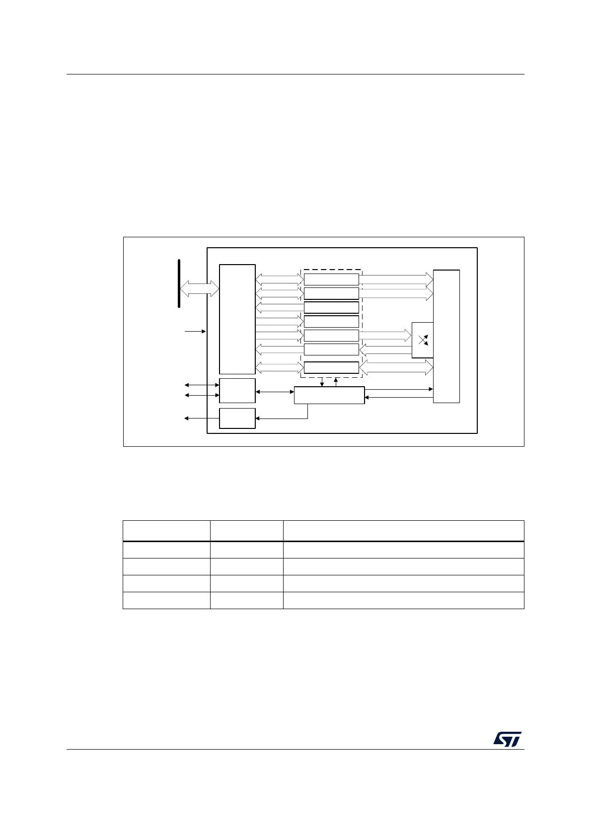
Figure 101 shows the block diagram of AES.
Figure 101. AES block diagram
23.4.2 AES internal signals
Table 133 describes the user relevant internal signals interfacing the AES peripheral.
MSv42154V1
aes_hclk
Banked registers
DOUT
KEY
IVI
DIN
AES
key
control
status
IV, counter
data in
data out
aes_it
32-bit
AHB bus
aes_in_dma
AES_CR
AES_KEYRx
AES_SR
AES_IVRx
AES_DINR
AES_DOUTR
AES
Core
(AEA)
swap
AHB
interface
IRQ
interface
Control Logic
DMA
interface
aes_out_dma
32-bit
access
Save / Restore
AES_SUSPRx
Table 133. AES internal input/output signals
Signal name Signal type Description
aes_hclk Input AHB bus clock
aes_it Output AES interrupt request
aes_in_dma Input/Output Input DMA single request/acknowledge
aes_out_dma Input/Output Output DMA single request/acknowledge