Public key accelerator (PKA) RM0453
696/1450 RM0453 Rev 5
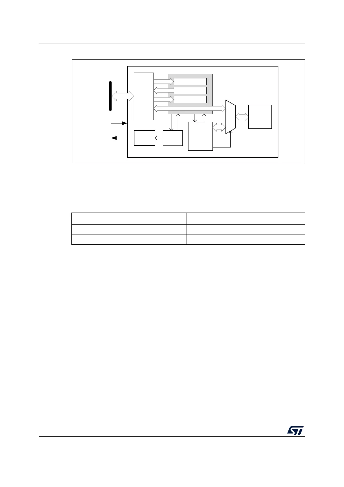
Figure 127. PKA block diagram
24.3.2 PKA internal signals
Table 143 lists internal signals available at the IP level, not necessarily available on product
bonding pads.
24.3.3 PKA reset and clocks
PKA is clocked on the AHB bus clock. The RAM receives this clock directly, the core is
clocked at half the frequency.
When the PKA peripheral reset signal is released PKA RAM is cleared automatically, taking
894 clock cycles. During this time the setting of EN bit in PKA_CR is ignored.
24.3.4 PKA public key acceleration
Overview
Public key accelerator (PKA) is used to accelerate Rivest, Shamir and Adleman (RSA),
Diffie-Hellman (DH) as well as ECC over prime field operations. Supported operand sizes is
up to 3136 bits for RSA and DH, and up to 640 bits for ECC.
The PKA supports all non-singular elliptic curves defined over prime fields, that can be
described with a short Weierstrass equation y
2
= x
3
+ ax + b (mod p). More information is
found in Section 24.5.1: Supported elliptic curves.
Note: Binary curves, Edwards curves and Curve25519 are not supported by the PKA.
A memory of 3576 bytes (894 words of 32 bits) called PKA RAM is used for providing initial
data to the PKA, and for holding the results after computation is completed. Access is done
though the PKA AHB interface.
MS45419V1
Banked registers (main)
PKA_CR
PKA core
control
status
Control
logic
894x32-bit
PKA RAM
IRQ
interface
PKA_CLRFR
clear
pka_it
pka_hclk
PKA32
32-bit access
32-bit
32-bit AHB bus
AHB
interface
PKA_SR
Table 143. Internal input/output signals
Signal name Signal type Description
pka_hclk Digital input AHB bus clock
pka_it Digital output Public key accelerator IP global interrupt request