General-purpose timers (TIM16/TIM17) RM0453
932/1450 RM0453 Rev 5
Note: The state of the external I/O pins connected to the complementary OCx and OCxN channels
depends on the OCx and OCxN channel state and GPIO control and alternate function
registers.
27.4.9 TIMx counter (TIMx_CNT)(x = 16 to 17)
Address offset: 0x24
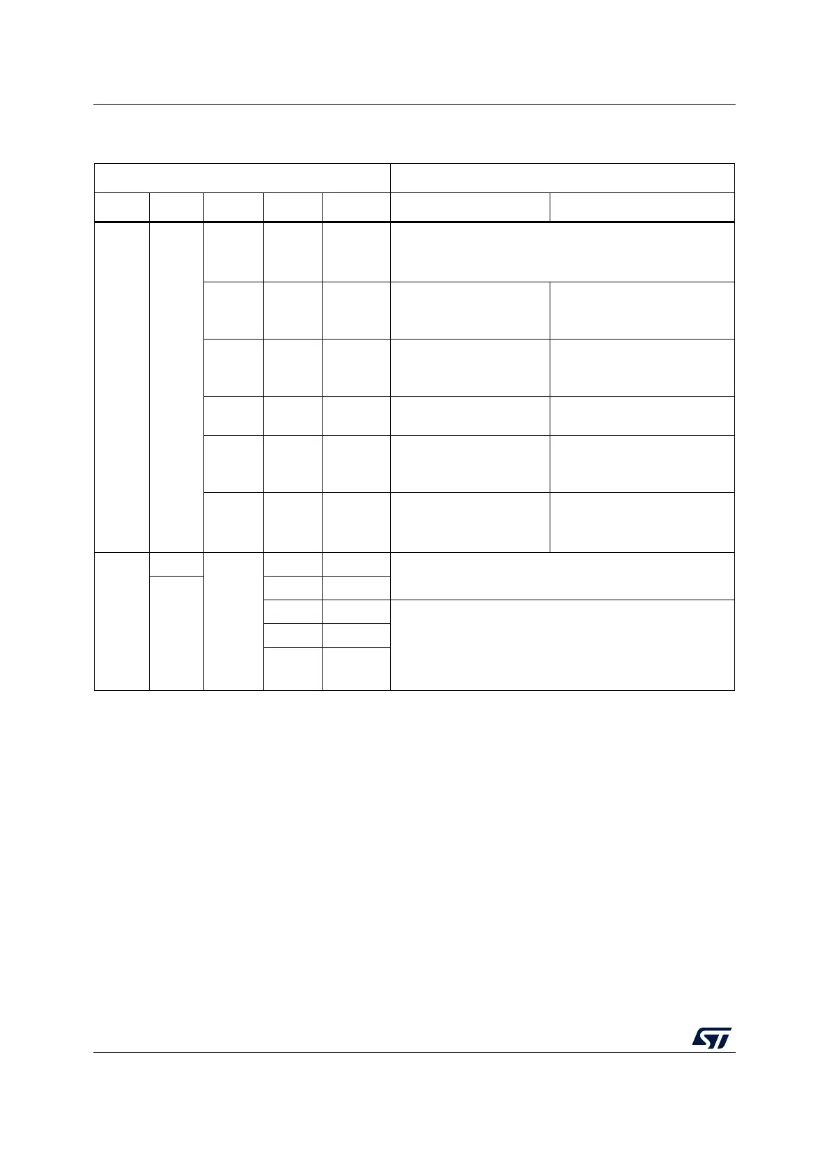
Table 187. Output control bits for complementary OCx and OCxN channels with break feature
(TIM16/17)
Control bits Output states
(1)
MOE bit OSSI bit OSSR bit CCxE bit CCxNE bit OCx output state OCxN output state
1X
X0 0
Output Disabled (not driven by the timer: Hi-Z)
OCx=0
OCxN=0, OCxN_EN=0
00 1
Output Disabled (not driven
by the timer: Hi-Z)
OCx=0
OCxREF + Polarity
OCxN=OCxREF XOR CCxNP
01 0
OCxREF + Polarity
OCx=OCxREF XOR CCxP
Output Disabled (not driven by
the timer: Hi-Z)
OCxN=0
X1 1
OCREF + Polarity + dead-
time
Complementary to OCREF (not
OCREF) + Polarity + dead-time
10 1
Off-State (output enabled
with inactive state)
OCx=CCxP
OCxREF + Polarity
OCxN=OCxREF XOR CCxNP
11 0
OCxREF + Polarity
OCx=OCxREF XOR CCxP,
OCx_EN=1
Off-State (output enabled with
inactive state)
OCxN=CCxNP, OCxN_EN=1
0
0
X
XX
Output disabled (not driven by the timer: Hi-Z).
1
00
0 1 Off-State (output enabled with inactive state)
Asynchronously: OCx=CCxP, OCxN=CCxNP
Then if the clock is present: OCx=OISx and OCxN=OISxN
after a dead-time, assuming that OISx and OISxN do not
correspond to OCX and OCxN both in active state
10
11
1. When both outputs of a channel are not used (control taken over by GPIO controller), the OISx, OISxN, CCxP and CCxNP
bits must be kept cleared.