RM0453 Rev 5 73/1450
RM0453
77
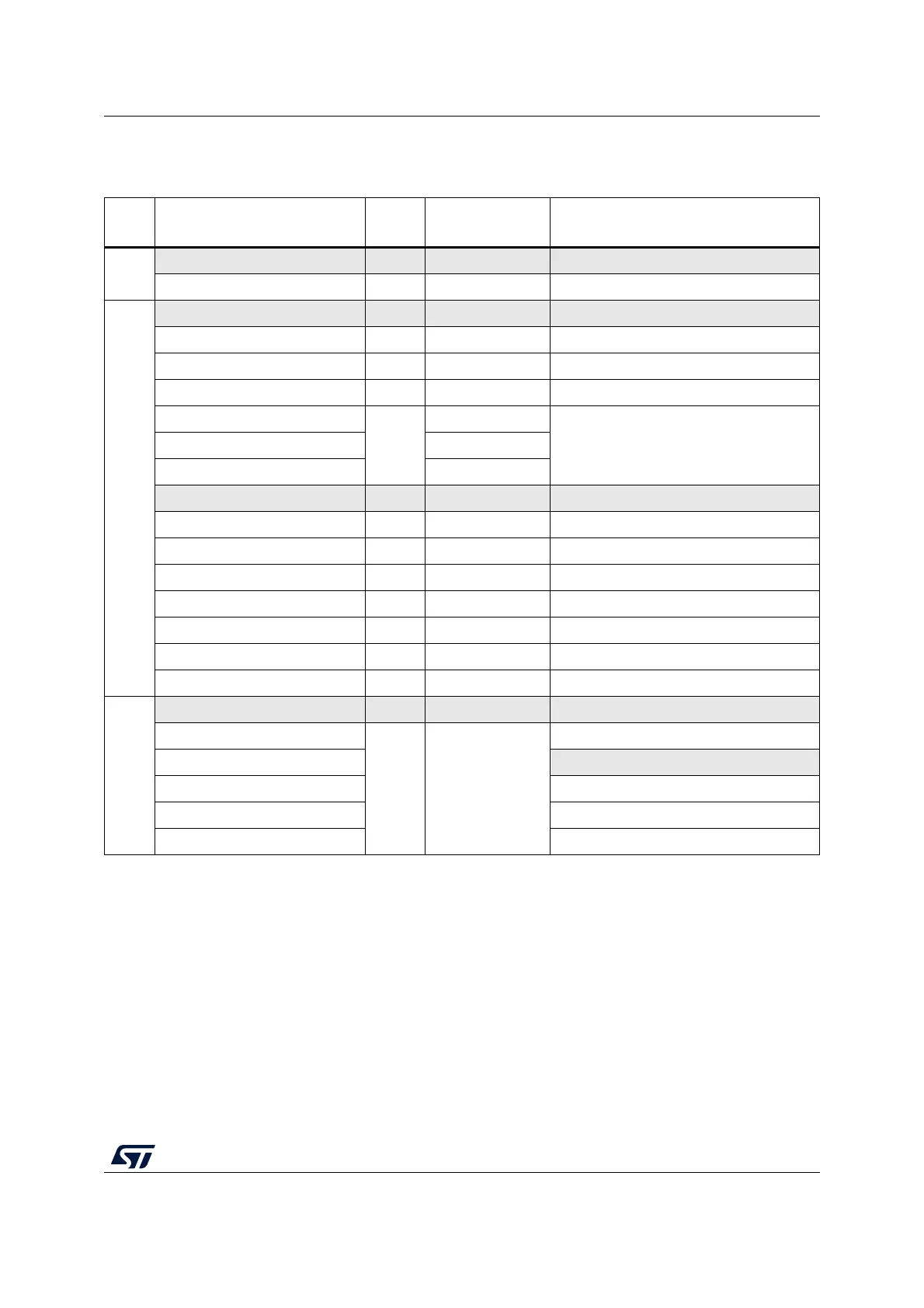
The table below details the boundary addresses of peripherals available in the device.
Table 4. Memory map and peripheral register boundary addresses
Bus Boundary address
Size
(bytes)
Peripheral Peripheral register map
APB3
0x5801 0400 - 0x5801 FFFF - Reserved -
0x5801 0000 - 0x5801 03FF 1 K SUBGHZSPI Section 37.9.10: SPI/I2S register map
AHB3
0x5800 40C0 - 0x5800 FFFF - Reserved -
0x5800 4800 - 0x5800 4BFF 1 K GTZC_TZIC Section 3.6.4: GTZC TZIC register map
0x5800 4400 - 0x5800 47FF 1 K GTZC_TZSC Section 3.5.8: GTZC TZSC register map
0x5800 4000 - 0x5800 43FF 1 K FLASH Section 4.10.21: FLASH register map
0x5800 3400 - 0x5800 3FFF
8 K
PKA continue
Section 24.7.5: PKA register map0x5800 2400 - 0x5800 33FF PKA RAM
0x5800 2000 - 0x5800 23FF PKA
0x5800 1C00 - 0x5800 1FFF - Reserved -
0x5800 1800 - 0x5800 1BFF 1 K AES Section 23.7.18: AES register map
0x5800 1400 - 0x5800 17FF 1 K HSEM Section 8.4.9: HSEM register map
0x5800 1000 - 0x5800 13FF 1 K True RNG Section 22.7.5: RNG register map
0x5800 0C00 - 0x5800 0FFF 1 K IPCC Section 9.4.9: IPCC register map
0x5800 0800 - 0x5800 0BFF 1 K EXTI Section 16.6.13: EXTI register map
0x5800 0400 - 0x5800 07FF 1 K PWR Section 6.6.23: PWR register map
0x5800 0000 - 0x5800 03FF 1 K RCC Section 7.4.47: RCC register map
AHB2
0x4800 2000 - 0x57FF FFFF - Reserved -
0x4800 1C00 - 0x4800 1FFF
8 K GPIO
Section 10.4.36: GPIOH register map
0x4800 0C00 - 0x4800 1BFF
Reserved
0x4800 0800 - 0x4800 0BFF Section 10.4.35: GPIOC register map
0x4800 0400 - 0x4800 07FF Section 10.4.34: GPIOB register map
0x4800 0000 - 0x4800 03FF Section 10.4.33: GPIOA register map