Low-power timer (LPTIM) RM0453
946/1450 RM0453 Rev 5
28.4 LPTIM functional description
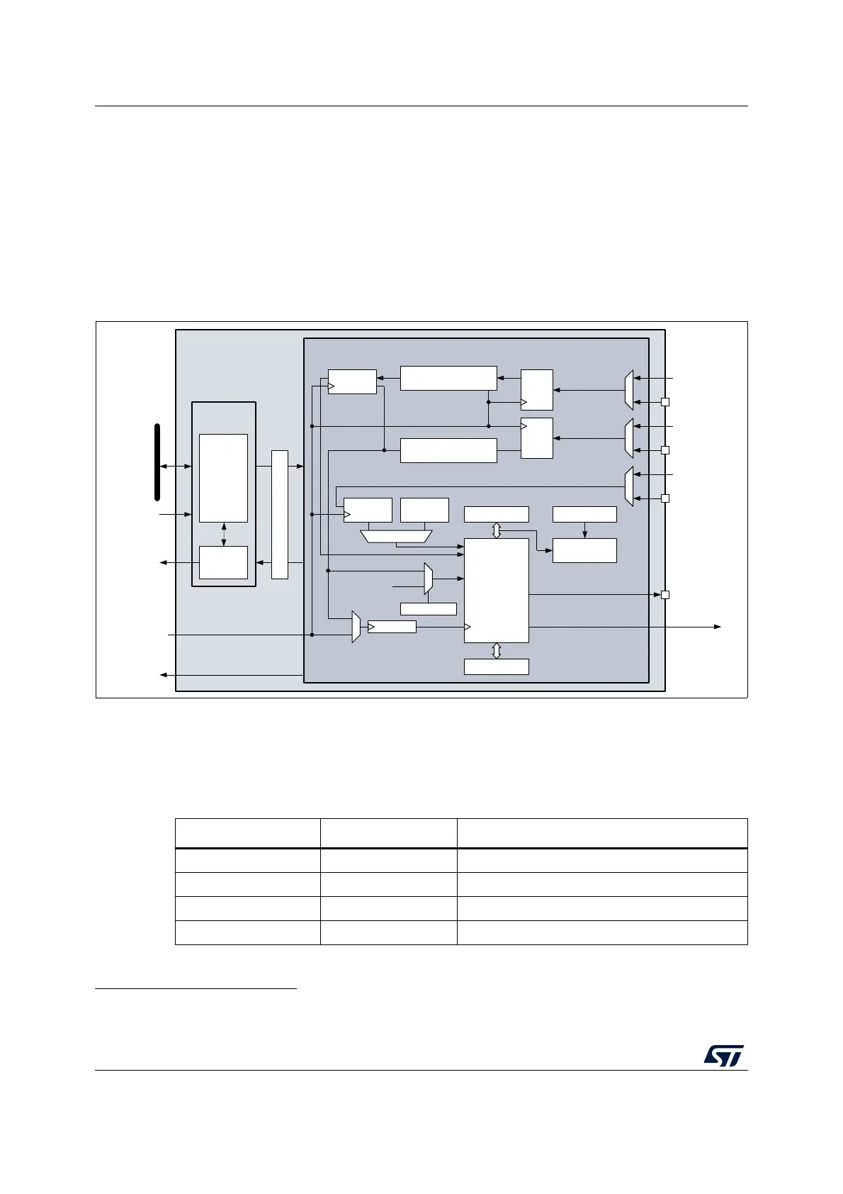
28.4.1 LPTIM block diagram
Figure 262. Low-power timer block diagram
(a)
1. lptim_out is the internal LPTIM output signal that can be connected to internal peripherals.
28.4.2 LPTIM pins and internal signals
The following tables provide the list of LPTIM pins and internal signals, respectively.
1. X = supported.
2. Wake-up supported from Stop 0, Stop 1 and Stop 2 modes.
3. Wake-up supported from Stop 0 and Stop 1 modes.
a. LPTIM2/LPTIM3 has only the input channel 1, no input channel 2.
MSv47413V3
LPTIM
Kernel clock domain
IRQ
interface
LPTIM
register
interface
APB clock
domain
32-bit APB bus
Wakeup
APB clock
LPTIM
interrupt
CLKMUX
16-bit counter
Count mode
16-bit compare
Repetition
counter
Prescaler
1
0
1
1
0
LPTIM_OUT
lptim_out
(1)
Synchronzation
16-bit ARR LPTIM_RCR
Mux trigger
Glitch
filter
CNTSTRT/
SNGSTRT
Glitch
filter
LPTIM_IN1
Encoder
Up/down
LPTIM_IN2
lptim_in2
lptim_in1
Glitch
filter
LPTIM_ETR
lptim_ext_trigx
Edge detector
Edge detector
lptim_ker_ck
Table 190. LPTIM input/output pins
Names Signal type Description
LPTIM_IN1 Digital input LPTIM Input 1 from GPIO pin
LPTIM_IN2 Digital input LPTIM Input 2 from GPIO pin
LPTIM_ETR Digital input LPTIM external trigger GPIO pin
LPTIM_OUT Digital output LPTIM Output GPIO pin