General-purpose timer (TIM2) RM0453
864/1450 RM0453 Rev 5
As in the previous example, both counters can be initialized before starting counting.
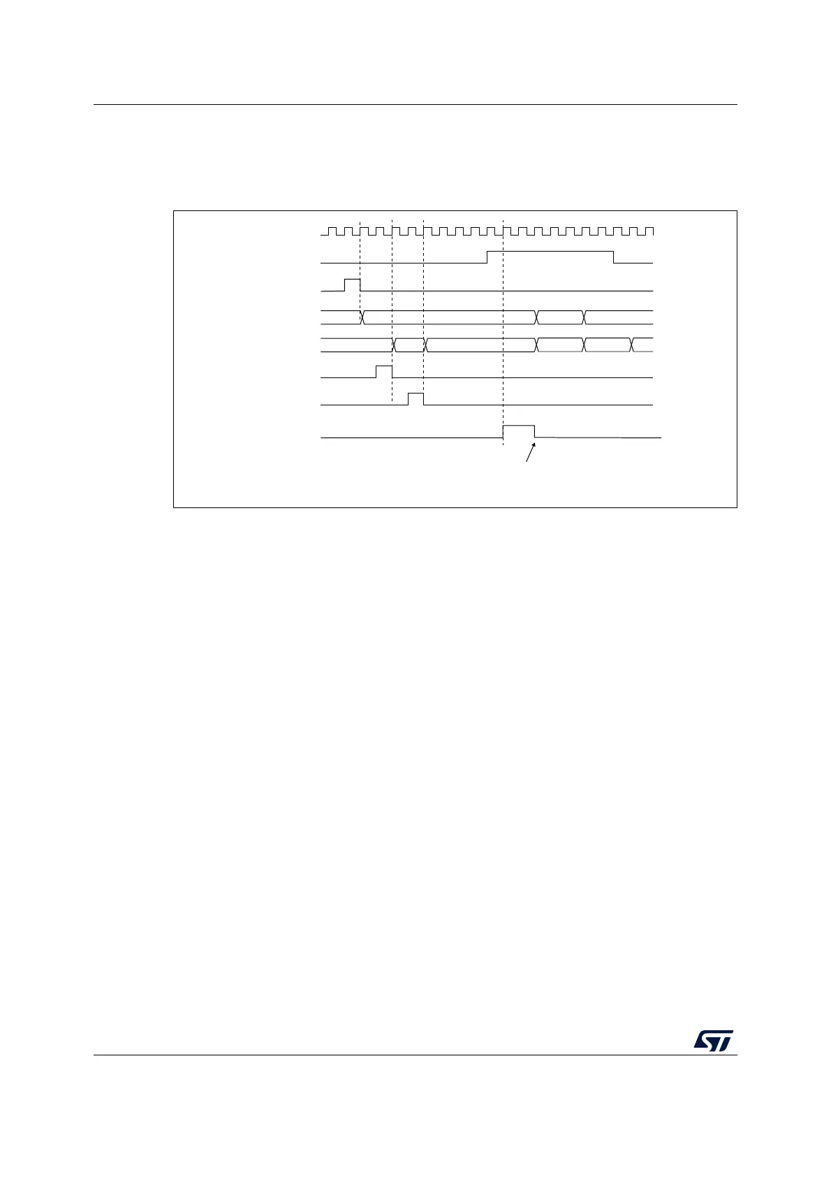
Figure 236 shows the behavior with the same configuration as in Figure 235 but in trigger
mode instead of gated mode (SMS=110 in the TIM2_SMCR register).
Figure 236. Triggering TIM2 with Enable of TIM1
Note: The clock of the slave peripherals (timer, ADC, ...) receiving the TRGO signal must be
enabled prior to receive events from the master timer, and the clock frequency (prescaler)
must not be changed on-the-fly while triggers are received from the master timer.
26.3.20 DMA burst mode
The TIMx timers have the capability to generate multiple DMA requests upon a single event.
The main purpose is to be able to re-program part of the timer multiple times without
software overhead, but it can also be used to read several registers in a row, at regular
intervals.
The DMA controller destination is unique and must point to the virtual register TIMx_DMAR.
On a given timer event, the timer launches a sequence of DMA requests (burst). Each write
into the TIMx_DMAR register is actually redirected to one of the timer registers.
The DBL[4:0] bits in the TIMx_DCR register set the DMA burst length. The timer recognizes
a burst transfer when a read or a write access is done to the TIMx_DMAR address), i.e. the
number of transfers (either in half-words or in bytes).
The DBA[4:0] bits in the TIMx_DCR registers define the DMA base address for DMA
transfers (when read/write access are done through the TIMx_DMAR address). DBA is
defined as an offset starting from the address of the TIMx_CR1 register:
Example:
00000: TIMx_CR1
00001: TIMx_CR2
00010: TIMx_SMCR
MS32698V1
CK_INT
TIM2-CNT
TIM1-CNT_INIT
Write TIF = 0
TIM1-CEN=CNT_EN
TIM2-TIF
E7
0200 01
E9
75
CD 00 E8 EA
TIM1-CNT
TIM2-CNT_INIT
TIM2
write CNT