Advanced-control timer (TIM1) RM0453
756/1450 RM0453 Rev 5
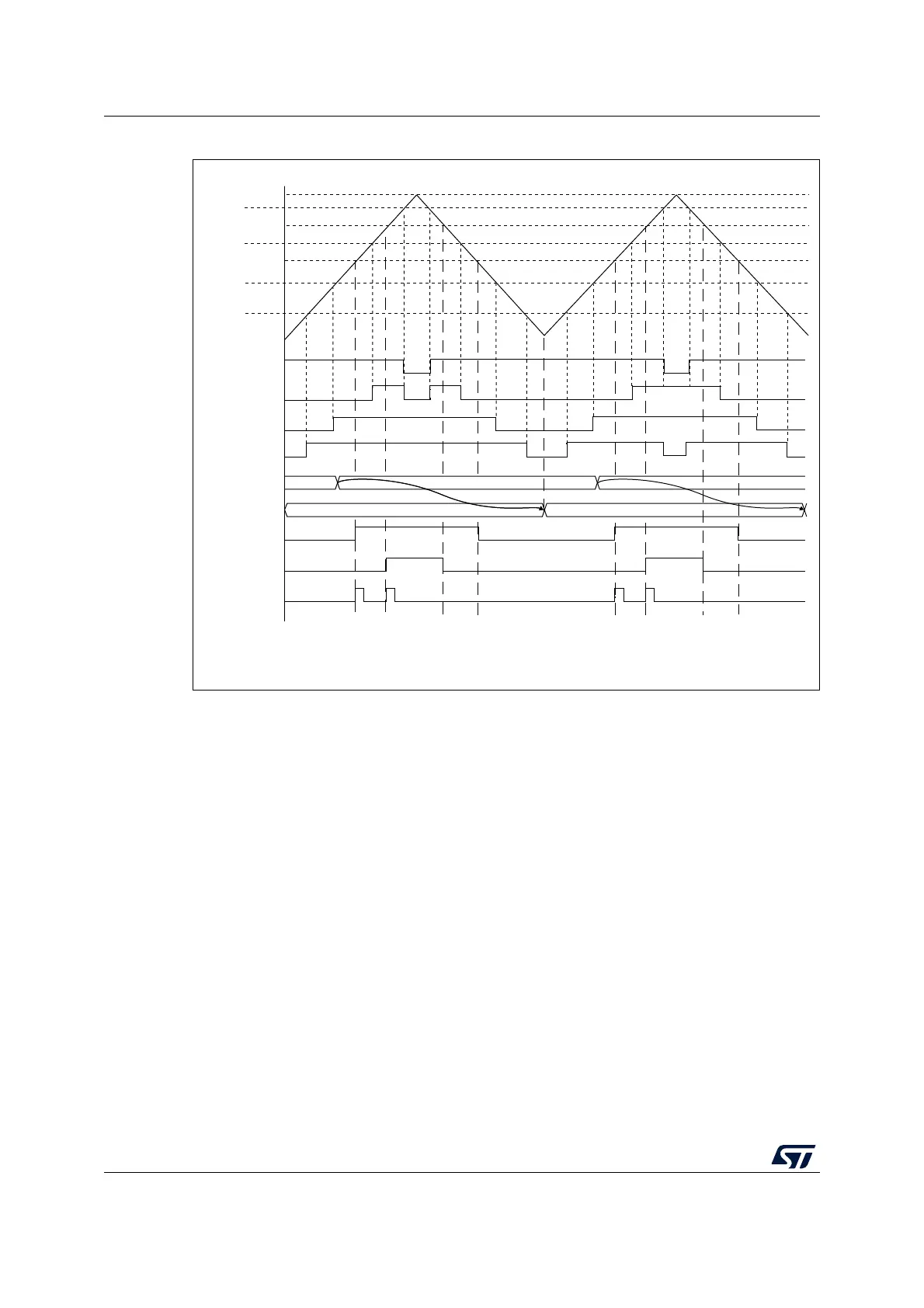
Figure 167. 3-phase combined PWM signals with multiple trigger pulses per period
The TRGO2 waveform shows how the ADC can be synchronized on given 3-phase PWM
signals. Refer to Section 25.3.27: ADC synchronization for more details.
25.3.15 Complementary outputs and dead-time insertion
The advanced-control timers (TIM1) can output two complementary signals and manage the
switching-off and the switching-on instants of the outputs.
This time is generally known as dead-time and it has to be adjusted depending on the
devices that are connected to the outputs and their characteristics (intrinsic delays of level-
shifters, delays due to power switches...)
The polarity of the outputs (main output OCx or complementary OCxN) can be selected
independently for each output. This is done by writing to the CCxP and CCxNP bits in the
TIMx_CCER register.
The complementary signals OCx and OCxN are activated by a combination of several
control bits: the CCxE and CCxNE bits in the TIMx_CCER register and the MOE, OISx,
OISxN, OSSI and OSSR bits in the TIMx_BDTR and TIMx_CR2 registers. Refer to
Table 180: Output control bits for complementary OCx and OCxN channels with break
feature on page 802 for more details. In particular, the dead-time is activated when
switching to the idle state (MOE falling down to 0).
ARR
OC5
OC1
OC2
OC3
OC5ref
OC1refC
OC6
OC4
TRGO2
100
xxx
001 100
Preload
GC5C[3:0]
xxx
Counter
MS33102V1
OC2refC
OC3refC
Active
OC4ref
OC6ref