Debug support (DBG) RM0453
1320/1450 RM0453 Rev 5
In the case of a FAULT or WAIT ACK response from the target, the data transfer phase is
canceled, unless overrun detection is enabled: in this case the data is ignored by the target
(in the case of a write), or not driven (in the case of a read).
A line reset must be generated by the host when it is first connected, or following a protocol
error. The line reset consists in 50 or more SWCLK cycles with SWDIO high, followed by
two SWCLK cycles with SWDIO low.
For more details on the Serial-wire debug protocol, refer to the Arm
®
Debug Interface
Architecture Specification [1].
Note: The SWJ-DP implements SWD protocol version 2.
38.4 Debug port (DP) registers
Both SW-DP and JTAG-DP access the DP registers listed in Table 268: DP register map
and reset values.
The debugger accesses the DP registers as follows:
• Program the A(3:2) field in the DPACC register, if using JTAG, with the register address
within the bank. Program the RnW bit to select a read or write. In the case of a write,
program the DATA field with the write data. If using SWD, the A(3:2) and RnW fields
are part of the packet request word sent to the SW-DP with the APnDP bit reset (see
Table 264). The write data are sent in the data phase.
• To access one of the banked DP registers at address 0x4, the register number must
first be written to the DP_SELECTR register at address 0x8. Any subsequent read or
write to address 0x4 accesses the register corresponding to the content of the
DP_SELECTR register.
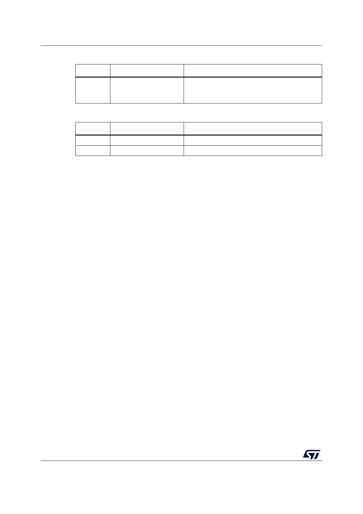
Table 265. ACK response
Bit field Name Description
2:0 ACK
– 000: FAULT
– 010: WAIT
– 100: OK
Table 266. Data transfer
Bit field Name Description
31:0 WDATA or RDATA Write or read data
32 Parity Single bit parity of 32 data bits