Digital-to-analog converter (DAC) RM0453
596/1450 RM0453 Rev 5
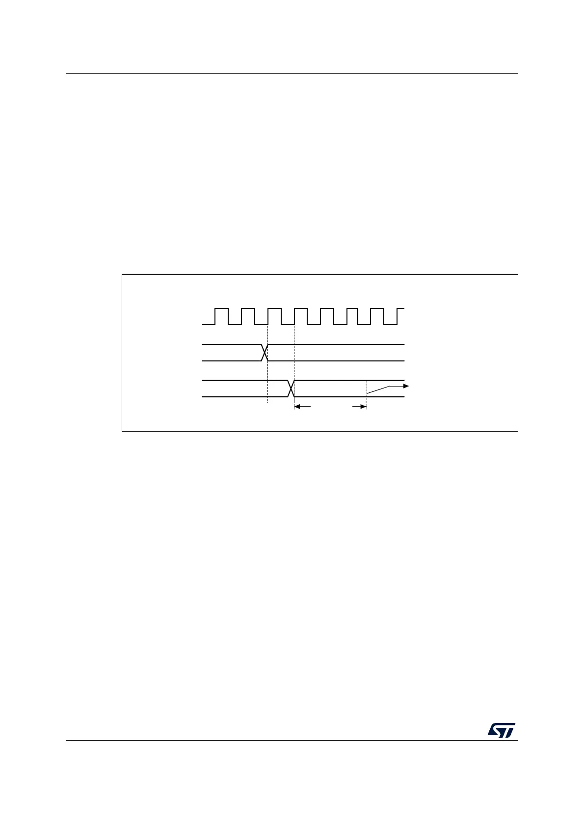
19.4.5 DAC conversion
The DAC_DOR1 cannot be written directly and any data transfer to the DAC channel1 must
be performed by loading the DAC_DHR1 register (write operation to DAC_DHR8R1,
DAC_DHR12L1, DAC_DHR12R1).
Data stored in the DAC_DHR1 register are automatically transferred to the DAC_DOR1
register after one dac_pclk clock cycle, if no hardware trigger is selected (TEN1 bit in
DAC_CR register is reset). However, when a hardware trigger is selected (TEN1 bit in
DAC_CR register is set) and a trigger occurs, the transfer is performed three dac_pclk clock
cycles after the trigger signal.
When DAC_DOR1 is loaded with the DAC_DHR1 contents, the analog output voltage
becomes available after a time t
SETTLING
that depends on the power supply voltage and the
analog output load.
Figure 88. Timing diagram for conversion with trigger disabled TEN = 0
19.4.6 DAC output voltage
Digital inputs are converted to output voltages on a linear conversion between 0 and V
REF+
.
The analog output voltage on the DAC channel pin is determined by the following equation:
19.4.7 DAC trigger selection
If the TEN1 control bit is set, the conversion can then be triggered by an external event (timer
counter, external interrupt line). The TSEL1[3:0] control bits determine which out of 16 pos-
sible events triggers the conversion as shown in TSEL1[3:0] bits of the DAC_CR register.
These events can be either the software trigger or hardware triggers. Refer to the intercon-
nection table in Section 19.4.2: DAC pins and internal signals.
Each time a DAC interface detects a rising edge on the selected trigger source (refer to the
table below), the last data stored into the DAC_DHR1 register are transferred into the
DAC_DOR1 register. The DAC_DOR1 register is updated three dac_pclk cycles after the
trigger occurs.
MSv45319V2
Bus clock
0x1AC
0x1AC
t
SETTLING
DHR
DOR
Output voltage available on
DAC_OUT pin
DACoutput V
REF
DOR
4096
--------------
×=