Debug support (DBG) RM0453
1328/1450 RM0453 Rev 5
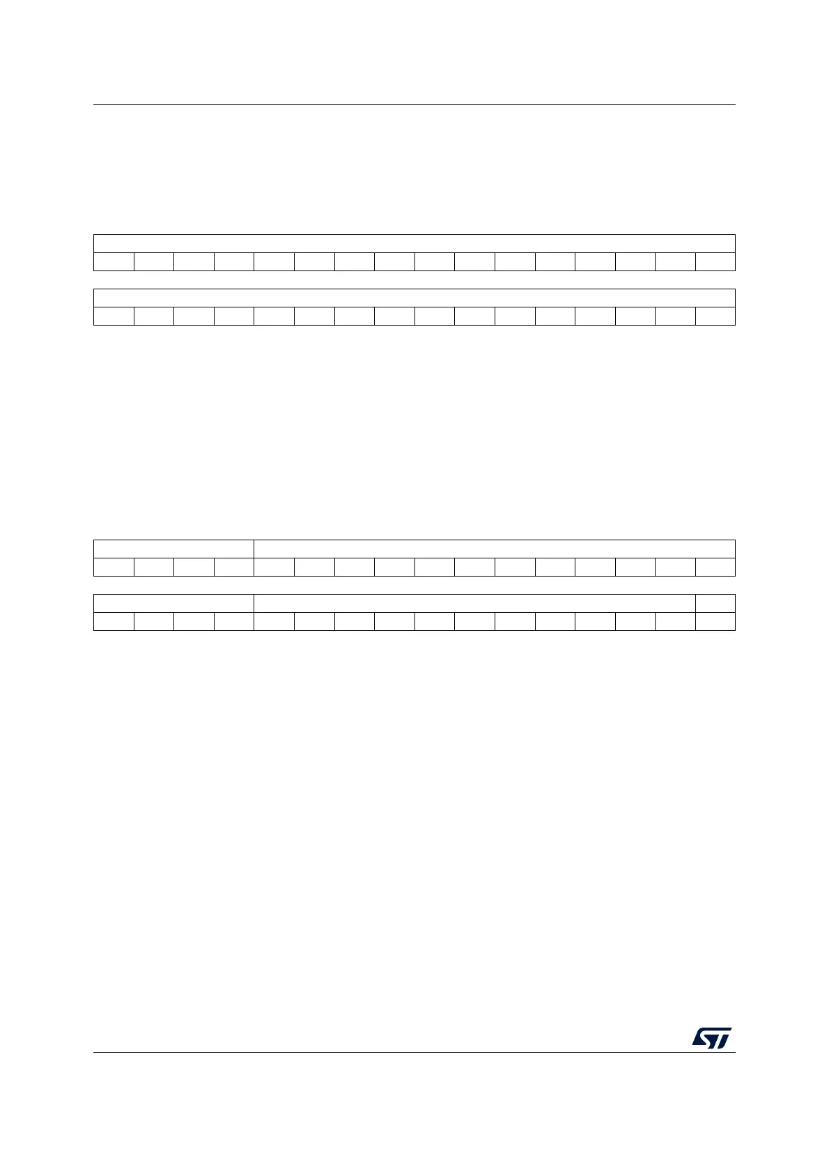
38.4.9 DP read buffer register (DP_BUFFR)
Address offset: 0x0C
Reset value: 0x0000 0000
38.4.10 DP target identification register (DP_TARGETSELR)
Address offset: 0x0C
Reset value: 0xXXXX XXXX
31 30 29 28 27 26 25 24 23 22 21 20 19 18 17 16
RDBUFF[31:16]
rrrrrrrrrrrrrrrr
1514131211109876543210
RDBUFF[15:0]
rrrrrrrrrrrrrrrr
Bits 31:0 RDBUFF[31:0]: Contains the value returned by the last AP read access.
The value returned by an AP read access can either be obtained using a second read access
to the same address, which initiates a new transaction on the corresponding bus, or else it
can be read from this register, in which case no new AP transaction occurs.
31 30 29 28 27 26 25 24 23 22 21 20 19 18 17 16
TINSTANCE[3:0] TPARTNO[15:4]
wwwwwwwwwwwwwwww
1514131211109876543210
TPARTNO[3:0] TDESIGNER[10:0] Res.
wwwwwwwwwwwwwww
Bits 31:28 TINSTANCE[3:0]: target instance number
Defines the instance number for the target device in a multi-drop system. These bits must be
written with the same value used for DP_DLPIDR.TINSTANCE to select this device.
Bits 27:12 TPARTNO[15:0]: target part number
Defines the part number for the target device. These bits must be written with the same value
used for DP_TARGETIDR.TPARTNO to select this device.
Bits 11:1 TDESIGNER[10:0]: target designer JEDEC code
Defines the JEDEC code for the target device. These bits must be written with the same
value used for DP_TARGETIDR.TDESIGNER to select this device.
Bit 0 Reserved, must be kept at reset value.