RM0453 Rev 5 629/1450
RM0453 Comparator (COMP)
631
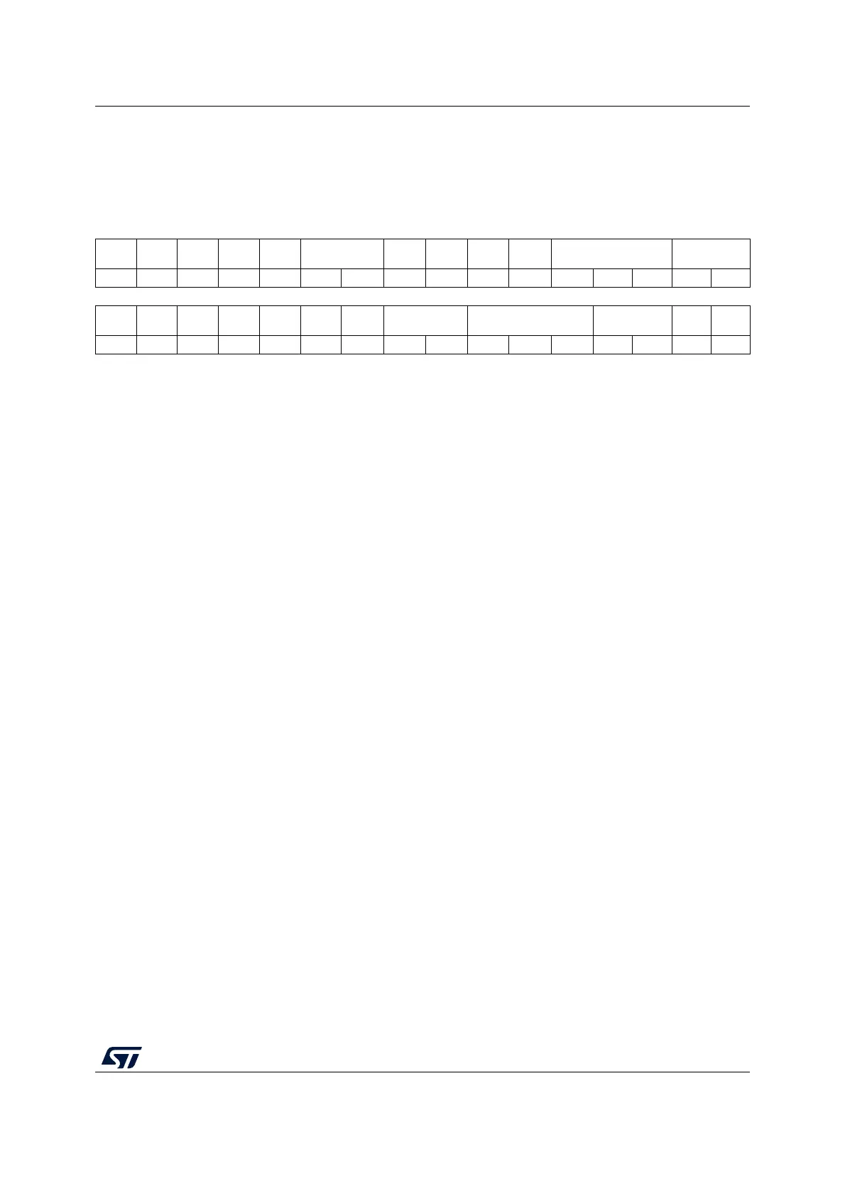
21.6.2 COMP2 control and status register (COMP2_CSR)
Address offset: 0x04
Reset value: 0x0000 0000
31 30 29 28 27 26 25 24 23 22 21 20 19 18 17 16
LOCK VALUE Res. Res. Res. INMESEL[1:0] Res.
SCAL
EN
BRGEN Res. BLANKING[2:0] HYST[1:0]
rsr rwrwrwrwrwrwrwrwrw
15 14 13 12 11 10 9 8 7 6 5 4 3 2 1 0
POLA
RITY
Res. Res. Res. Res. Res.
WIN
MODE
INPSEL[1:0] INMSEL[2:0] PWRMODE[1:0] Res. EN
rw rw rw rw rw rw rw rw rw rw
Bit 31 LOCK: locks the whole content of the register, COMP2_CSR[31:0]
This bit is set by software and cleared by a hardware system reset.
0: COMP2_CSR[31:0] are read/write.
1: COMP2_CSR[31:0] are read-only.
Bit 30 VALUE: COMP2 output status bit
This bit is read-only. It reflects the current COMP2 output taking into account the effect of the
POLARITY bit.
Bits 29:27 Reserved, must be kept at reset value.
Bits 26:25 INMESEL[1:0]: COMP2 input minus extended selection
These bits are set and cleared by software. They select which extended GPIO input is
connected to the input minus of COMP2, if INMSEL[2:0] = 111.
00: PB2
01: PA10
10: PA11
11: reserved
Bit 24 Reserved, must be kept at reset value.
Bit 23 SCALEN: voltage scaler enable
This bit is set and cleared by software. It enables outputs of the V
REFINT
divider available on
the minus input of COMP2.
0: Bandgap scaler disabled (if SCALEN bit of COMP1_CSR register is also reset)
1: Bandgap scaler enabled
Bit 22 BRGEN: scaler bridge enable
This bit is set and cleared by software. It enables the bridge of the scaler.
If SCALEN is set and BRGEN is reset, the BG voltage reference is available but not 1/4
BGAP, 1/2 BGAP or 3/4 BGAP. The BGAP value is sent instead of 1/4 BGAP, 1/2 BGAP, 3/4
BGAP. If SCALEN and BRGEN are both set, 1/4 BGAP 1/2 BGAP 3/4 BGAP and BGAP
voltage references are available.
0: Scaler resistor bridge disabled (if BRGEN bit of COMP1_CSR register is also reset)
1: Scaler resistor bridge enabled
Bit 21 Reserved, must be kept at reset value.