General-purpose timers (TIM16/TIM17) RM0453
928/1450 RM0453 Rev 5
27.4.7 TIMx capture/compare mode register 1 [alternate]
(TIMx_CCMR1)(x = 16 to 17)
Address offset: 0x18
Reset value: 0x0000 0000
The same register can be used for output compare mode (this section) or for input capture
mode (previous section). The direction of a channel is defined by configuring the
corresponding CCxS bits. All the other bits of this register have a different function in input
and in output mode.
Output compare mode:
Bits 1:0 CC1S[1:0]: Capture/Compare 1 Selection
This bit-field defines the direction of the channel (input/output) as well as the used input.
00: CC1 channel is configured as output
01: CC1 channel is configured as input, IC1 is mapped on TI1
Others: Reserved
Note: CC1S bits are writable only when the channel is OFF (CC1E = ‘0’ in TIMx_CCER).
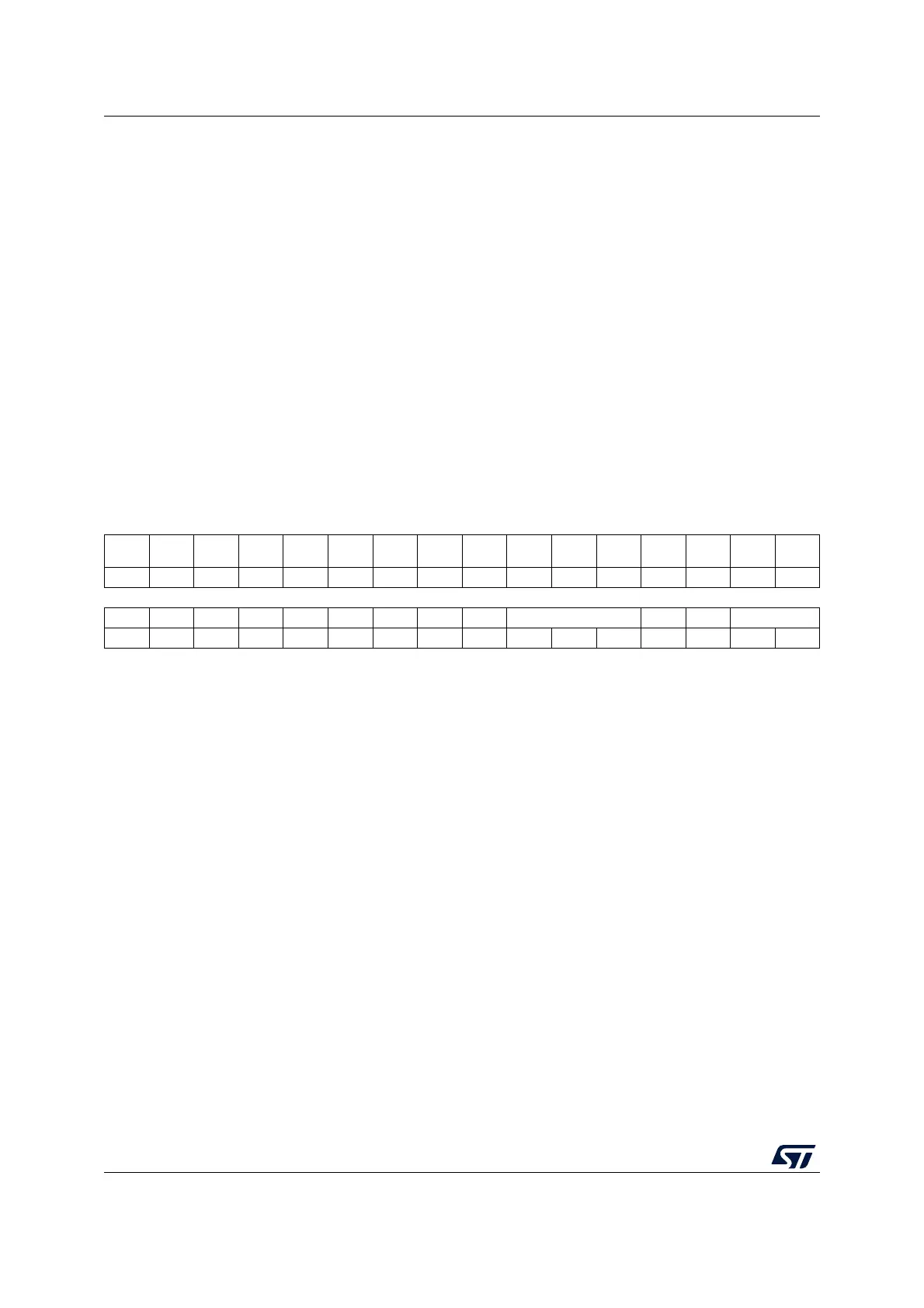
31 30 29 28 27 26 25 24 23 22 21 20 19 18 17 16
Res. Res. Res. Res. Res. Res. Res. Res. Res. Res. Res. Res. Res. Res. Res.
OC1M
[3]
rw
1514131211109876543210
Res. Res. Res. Res. Res. Res. Res. Res. Res. OC1M[2:0] OC1PE OC1FE CC1S[1:0]
rw rw rw rw rw rw rw
Bits 31:17 Reserved, must be kept at reset value.
Bits 15:7 Reserved, must be kept at reset value.