13. USING STO FUNCTION
13 - 11
13.4 Detailed description of interfaces
This section provides the details of the I/O signal interfaces (refer to the I/O division in the table) given in
section 13.2. Refer to this section and make connection with the external device.
13.4.1 Sink I/O interface
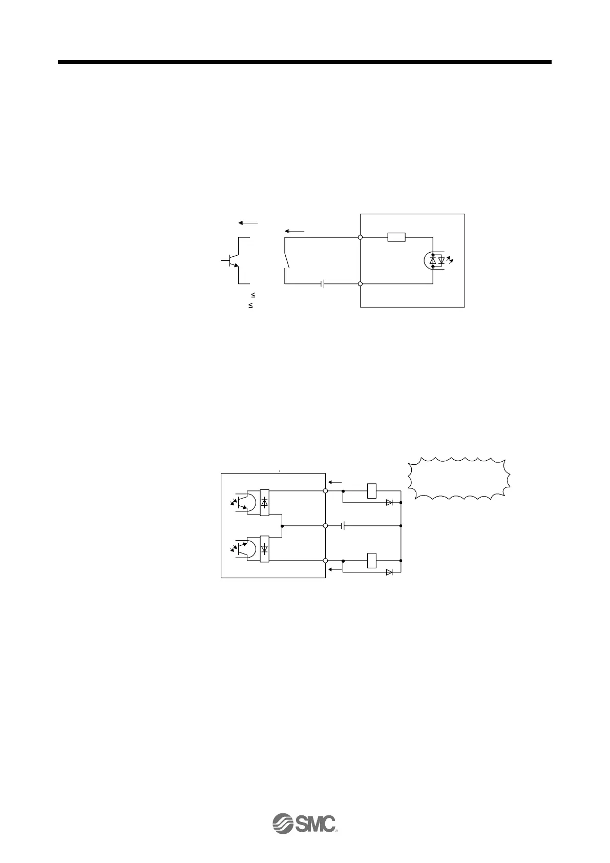
(1) Digital input interface DI-1
This is an input circuit whose photocoupler cathode side is input terminal. Transmit signals from sink
(open-collector) type transistor output, relay switch, etc.
Approx. 3.0 kΩ
STO1
STO2
Servo amplifier
Sw itch
Approx. 5 mA
For transistor
STOCOM
TR
V
CES
1.0 V
I
CEO
100 µA
24 V DC ± 10%
300 mA
(2) Digital output interface DO-1
This is a circuit of collector output terminal of the output transistor. When the output transistor is
turned on, collector terminal current will be applied for the output.
A lamp, relay or photocoupler can be driven. Install a diode (D) for an inductive load, or install an
inrush current suppressing resistor (R) for a lamp load.
(Rated current: 40 mA or less, maximum current: 50 mA or less, inrush current: 100 mA or less) A
maximum of 5.2 V voltage drop occurs in the driver.
(a) When outputting two STO states by using each TOFB
TOFCOM
Servo amplifier
TOFB2
If polarity of diode is
reversed, servo amplifier
w ill malfunction.
LoadTOFB1
Load
(Note)
24 V DC ± 10%
300 mA
If the voltage drop (maximum of 2.6 V) interferes with the relay operation, apply high
voltage (maximum of 26.4 V) from external source.
 Loading...