Parameter Value
Conversion time 1 ms (none),
100 ms (50 Hz / 60 Hz) per channel
Resolution Ran
ge
unipolar 15 bits
bipolar 15 bits + sign
Conversion error of the analog values caused by
non-linearity, adjustment error at factory and resolu-
tion within the normal range
Typ. ±0.1 % (voltage)
±0.3 % (current, resistor)
at 25 °C
Max
.
±0.7 % (voltage)
±0.9 % (current, resistor)
±0.5 % (thermocouple type J, N,
S, T; thermocouple type K > -220
°C)
1.0 K (resistance temperature
detectors)
at 0 °C...60 °C or EMC disturb-
ance
Maximum permanent allowed overload (no damage)
Current input When the input current exceeds the
overflow value of the measurement
range, the input impedance is switched
to high impedance for protection. The
maximum allowed overload is then 30
V. The digital value corresponds to the
overflow value. Periodically, the input
impedance is switched to the normal
value and the input current is measured.
If the input current is within the meas-
urement range, the input impedance
remains at the normal level and the dig-
ital value corresponds to the measured
current.
Voltage input 30 V
Relationship between input signal and hex code
Ä
Table 94 “Channel monitoring”
on page 475
Unused voltage inputs Are configured as "unused"
Unused current inputs Have a low resistance, can be left open-
circuited
Overvoltage protection Yes
Technical data of the analog inputs if used as digital inputs
Parameter Value
Number of channels per module Max. 8
Distribution of channels into groups 2 groups of 4 channels each
Connections of the channels I0+ to I3+
Connections of the channels I4+ to I7+
Terminals 2.0, 2.2, 2.4, 2.6
Terminals 4.0, 4.2, 4.4, 4.6
Reference potential for the inputs Terminals 1.9, 2.9, 3.9 and 4.9 (ZP)
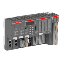
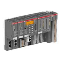
I/O modules > Analog I/O modules
2022/01/313ADR010278, 3, en_US484