Parameter Value
Resistance to feedback against 24 V signals Yes (software-controlled supervision)
Max. cable length
Shielded 1000 m
Unshielded 600 m
The following drawing shows the circuitry of a digital input/output with the varistors for demag-
netization when inductive loads are switched off.
Fig. 149: Digital input/output (circuit diagram)
1 Digital Output
2 Varistors for demagnetization when inductive loads are turned off
Technical data of the analog inputs
Parameter Value
Number of channels per module 4
Distribution of channels into groups 1 group with 4 channels
Connection if channels AI0+ to AI3+ Terminals 1.0 to1.3
Reference potential for AI0+ to AI3+ Terminal 1.4 (AI-) for voltage and RTD meas-
urement
Terminal 1.9, 2.9 and 3.9 for current measure-
ment
Input type
Unipolar Voltage 0 ... 10 V, current or Pt100/Pt1000/
Ni1000
Bipolar Voltage -10 ... +10 V
Galvanic isolation Against Ethernet network
Configurability 0...10 V, -10...+10 V, 0/4...20 mA, Pt100/1000,
Ni1000 (each input can be configured individu-
ally)
Channel input resistance Voltage: > 100 kW
Current: ca. 330 W
Time constant of the input filter Voltage: 100 µs
Current: 100 µs
Indication of the input signals 1 LED per channel (brightness depends on the
value of the analog signal)
Conversion cycle 1 ms (for 4 inputs + 2 outputs); with RTDs Pt/
Ni... 1 s
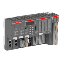
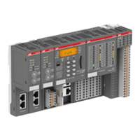
Communication interface modules (S500) > Modbus
2022/01/313ADR010278, 3, en_US766