RM0453 Rev 5 439/1450
RM0453 System configuration controller (SYSCFG)
445
11.2.9 SYSCFG SRAM2 write protection register (SYSCFG_SWPR)
Address offset: 0x020
Reset value: 0x0000 0000
Bits 7:4 Reserved, must be kept at reset value.
Bit 3 ECCL: ECC lock
This bit is set by software and cleared only by a system reset. It can be used to enable and
lock the flash ECC error connection to TIM1/16/17 break input.
0: ECC error disconnected from TIM1/16/17 break input.
1: ECC error connected to TIM1/16/17 break input.
Bit 2 PVDL: PVD lock enable bit
This bit is set by software and cleared only by a system reset. It can be used to enable and
lock the PVD connection to TIM1/16/17 break input, as well as the PVDE and PLS[2:0] in the
PWR_CR2R register.
0: PVD interrupt disconnected from TIM1/16/17 break input. PVDE and PLS[2:0] bits can be
programmed by the application.
1: PVD interrupt connected to TIM1/16/17 break input. PVDE and PLS[2:0] bits are read only.
Bit 1 SPL: SRAM2 parity lock bit
This bit is set by software and cleared only by a system reset. It can be used to enable and
lock the SRAM2 parity error signal connection to TIM1/16/17 break inputs.
0: SRAM2 parity error signal disconnected from TIM1/16/17 break inputs
1: SRAM2 parity error signal connected to TIM1/16/17 break inputs
Bit 0 CLL: CPU1 LOCKUP (Hardfault) output enable bit
This bit is set by software and cleared only by a system reset. It can be used to enable and
lock the connection of CPU1 LOCKUP (Hardfault) output to TIM1/16/17 break inputs.
0: CPU1 LOCKUP output disconnected from TIM1/16/17 break inputs
1: CPU1 LOCKUP output connected to TIM1/16/17 break inputs
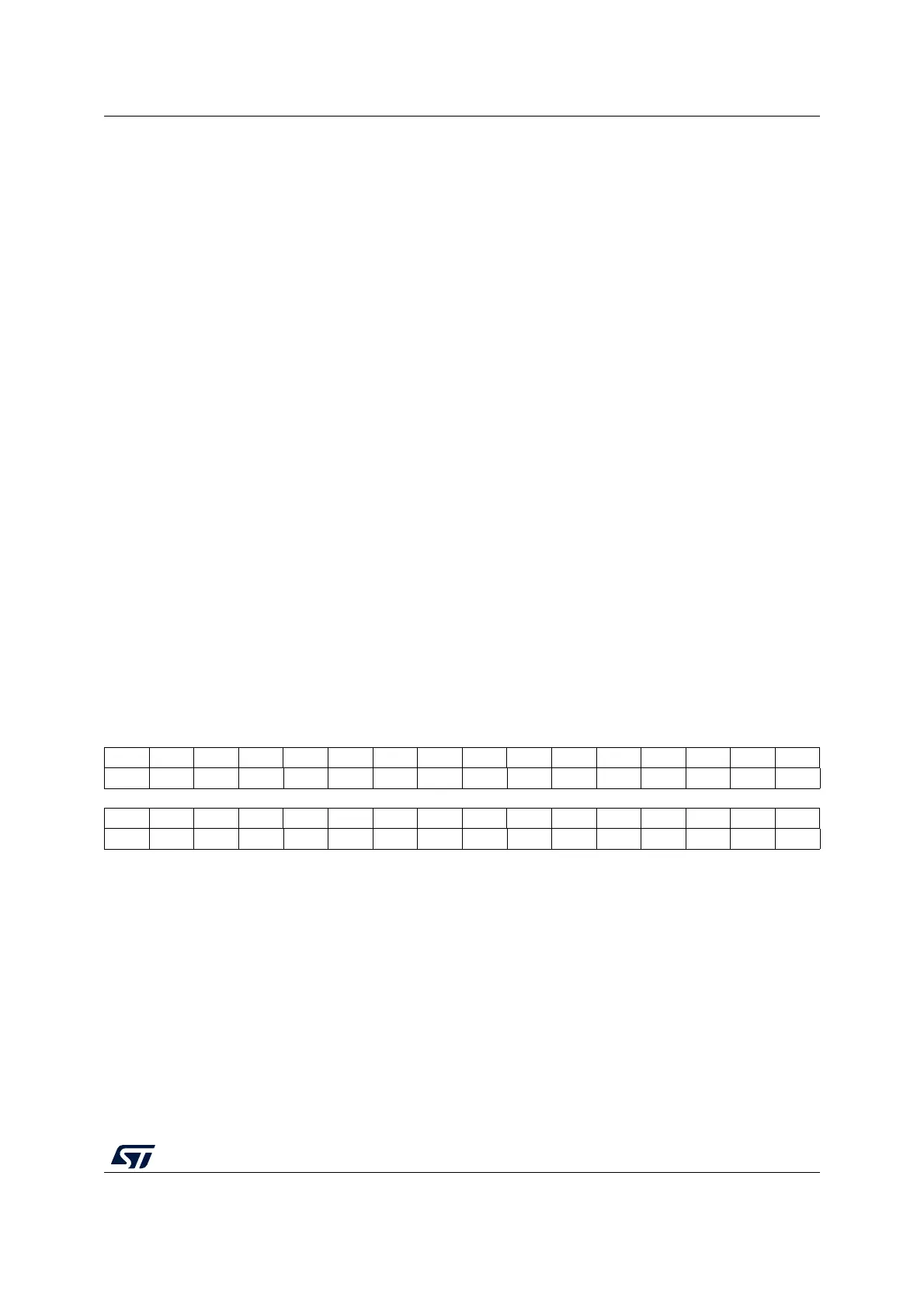
31 30 29 28 27 26 25 24 23 22 21 20 19 18 17 16
P31WP P30WP P29WP P28WP P27WP P26WP P25WP P24WP P23WP P22WP P21WP P20WP P19WP P18WP P17WP P16WP
rs rs rs rs rs rs rs rs rs rs rs rs rs rs rs rs
1514131211109876543210
P15WP P14WP P13WP P12WP P11WP P10WP P9WP P8WP P7WP P6WP P5WP P4WP P3WP P2WP P1WP P0WP
rs rs rs rs rs rs rs rs rs rs rs rs rs rs rs rs
Bits 31:0 PxWP: SRAM2 1 Kbyte page x write protection (x = 31 to 0)
These bits are set by software and cleared only by a system reset.
0: Write protection of SRAM2 1 Kbyte page x is disabled.
1: Write protection of SRAM2 1 Kbyte page x is enabled.