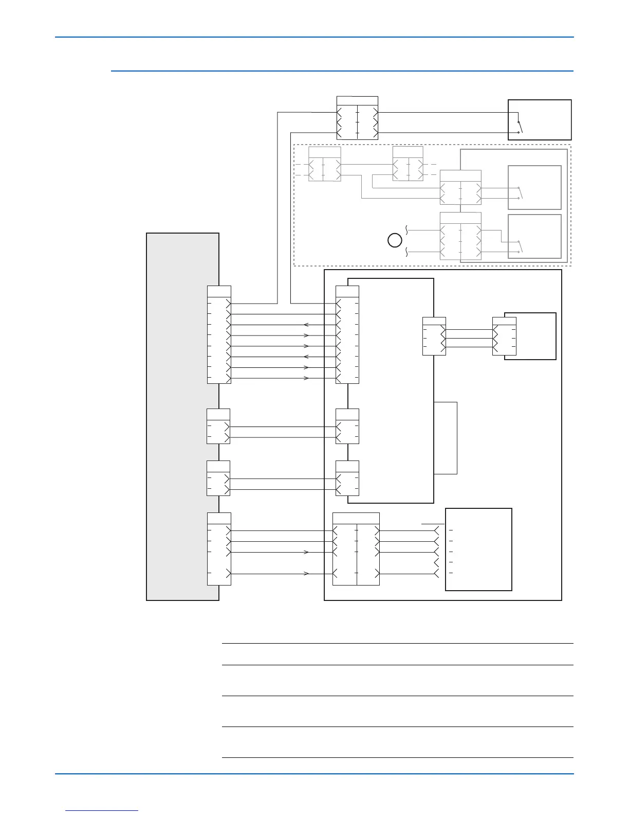
Phaser 4500/4510 Service Manual 10-29
Wiring Diagrams
Laser Unit, 5 V Interlock, Interlock Switch Assembly
Signal line name Description
/SOS Synchronization signal generated by SOS Sensor. This signal
commands start of each scan.
/PCONT Sample / Hold circuit
Low: Sampled (LD is forcibly lit up); High: Held
Vref Laser output control signal for determining or adjusting the
current flowing through Laser Diode.
P/J130
Start Of
Scan
Sensor
HVPS/
Engine Logic
PWBA
LVPS Harness
5/6
Laser Unit
Harness
2
3
4
5
6
7
8
1
2
3
4
1
7
6
5
4
3
2
1
8
SG
/SOS
N.C.
N.C. N.C.
N.C.
/PCONT 1
Vref
MO/DET-OUT
/PCONT2
/LDENB
XPDATA 2+
XPDATA 2-
P/J14
P/J140
1
2
P/J170
2
3
1
5VDC AFT
Laser Unit
Laser Diode
Scanner
Motor
/SOS
SG
2
1
3
2
1
P/J17
XPDATA 1+
XPDATA 1-
24V DC
24V RTN/SG
/ROSMOT ON
/ROSMOT CLK
1
2
P/J160
2
1
P/J16
P/J13
4
3
2
1
5
2
2
1
3
4
3
4
1
P/J131
3
2
1
1
3
2
P/J141
5V Interlock
Laser
Interlock
Top Cover
Switch
2
1
1
2
P/J141
2
1
1
2
P/J142
P/J201 P/J2011
s4510-239
Interlock Switch Assembly
2
1
1
2
P/J144
3
1
1
3
P/J411
22
A
5 V DC
P4500 Only
To page 10-21
 Loading...