MPC5553/MPC5554 Microcontroller Reference Manual, Rev. 5
24-6 Freescale Semiconductor
24.3.1.4 Boundary Scan Register
The boundary scan register is connected between TDI and TDO when the EXTEST, SAMPLE or
SAMPLE/PRELOAD instructions are active. It is used to capture input pin data, force fixed values on
output pins, and select a logic value and direction for bidirectional pins. Each bit of the boundary scan
register represents a separate boundary scan register cell, as described in the IEEE 1149.1-2001 standard
and discussed in Section 24.4.5, “Boundary Scan.” The size of the boundary scan register is 464 bits for
the MPC5554, and 392 bits for the MPC5553.
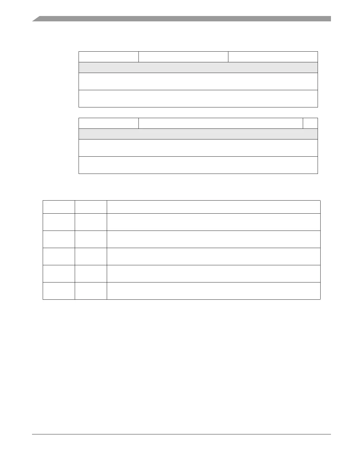
0123456789101112131415
R PRN DC PIN
W
Reset
MPC5553
0000100000000101
Reset
MPC5554
0000100000000000
16 17 18 19 20 21 22 23 24 25 26 27 28 29 30 31
RPIN MIC 1
W
Reset
MPC5553
0011000000011101
Reset
MPC5554
0000000000011101
Figure 24-3. Device Identification Register
Table 24-2. Device Identification Register Field Descriptions
Bits Name Description
0–3 PRN Part revision number. Contains the revision number of the device. This field changes with
each revision of the device or module.
4–9 DC Design center. Indicates the Freescale design center. For both the MPC5554 and
MPC5553, this value is 0x20.
10–19 PIN Part identification number. Contains the part number of the device. For the MPC5554, this
value is 0x0, for the MPC5553 this value is 0x53.
20–30 MIC Manufacturer identity code. Contains the reduced Joint Electron Device Engineering
Council (JEDEC) ID for Freescale, 0xE.
31 — IDCODE register ID. Identifies this register as the device identification register and not the
bypass register. Always set to 1.