MPC5553/MPC5554 Microcontroller Reference Manual, Rev. 5
15-2 Freescale Semiconductor
15.2.2.1 Data Retention
Updates to the standby portion of SRAM are not performed during system reset or standby mode.
15.3 External Signal Description
The only external signal used by the SRAM is the V
STBY
RAM power supply. If external SRAM is not
used, tie V
STBY
to V
SS
.
15.4 Memory Map/Register Definition
SRAM occupies 64 KB of address space as shown in Table 1-2. Table 15-1 shows the SRAM memory
map.
15.4.1 Register Descriptions
The internal SRAM has no registers. Registers associated with the SRAM ECC are located in the ECSM.
Refer to Section 8.2.1, “Register Descriptions.”
15.5 Functional Description
The ECC checks are performed during the read portion of an SRAM ECC read/write (R/W) operation, and
ECC calculations are performed during the write portion of a read/write (R/W) operation.
Because the ECC bits can contain random data after the device is powered on, the user must initialize the
SRAM by executing 64-bit write instructions to the entire SRAM. For more information, refer to
Section 15.7, “Initialization/Application Information.”
15.6 SRAM ECC Mechanism
The SRAM ECC detects the following conditions and produces the following results:
— Detects and corrects all 1-bit errors
— Detects and flags all 2-bit errors as non-correctable errors
— Detects 72-bit reads (64-bit data bus plus the 8-bit ECC) that return all zeros or all ones, asserts
an error indicator on the bus cycle, and sets the multiple-bit error flag
SRAM does not detect all errors greater than 2-bits.
Internal SRAM write operations are performed on the following byte boundaries:
— 1 byte (0:7 bits)
— 2 bytes (0:15 bits)
— 4 bytes or 1 word (0:31 bits)
— 8 bytes or 2 words (0:63 bits)
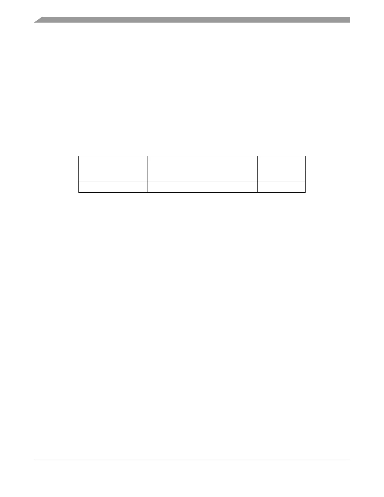
Table 15-1. SRAM Memory Map
Address Register Description Size
Base (0x4000_0000) 32 KB RAM powered by V
STBY
32 KB
Base + 0x8000 32 KB RAM 32 KB