MPC5553/MPC5554 Microcontroller Reference Manual, Rev. 5
Freescale Semiconductor 19-103
19.4.9 Analog Submodule
19.4.9.1 Reference Bypass
The reference bypass capacitor (REFBYPC) signal requires a 100 nF capacitor connected to VRL to filter
noise on the internal reference used by the ADC.
Figure 19-59. Reference Bypass Circuit
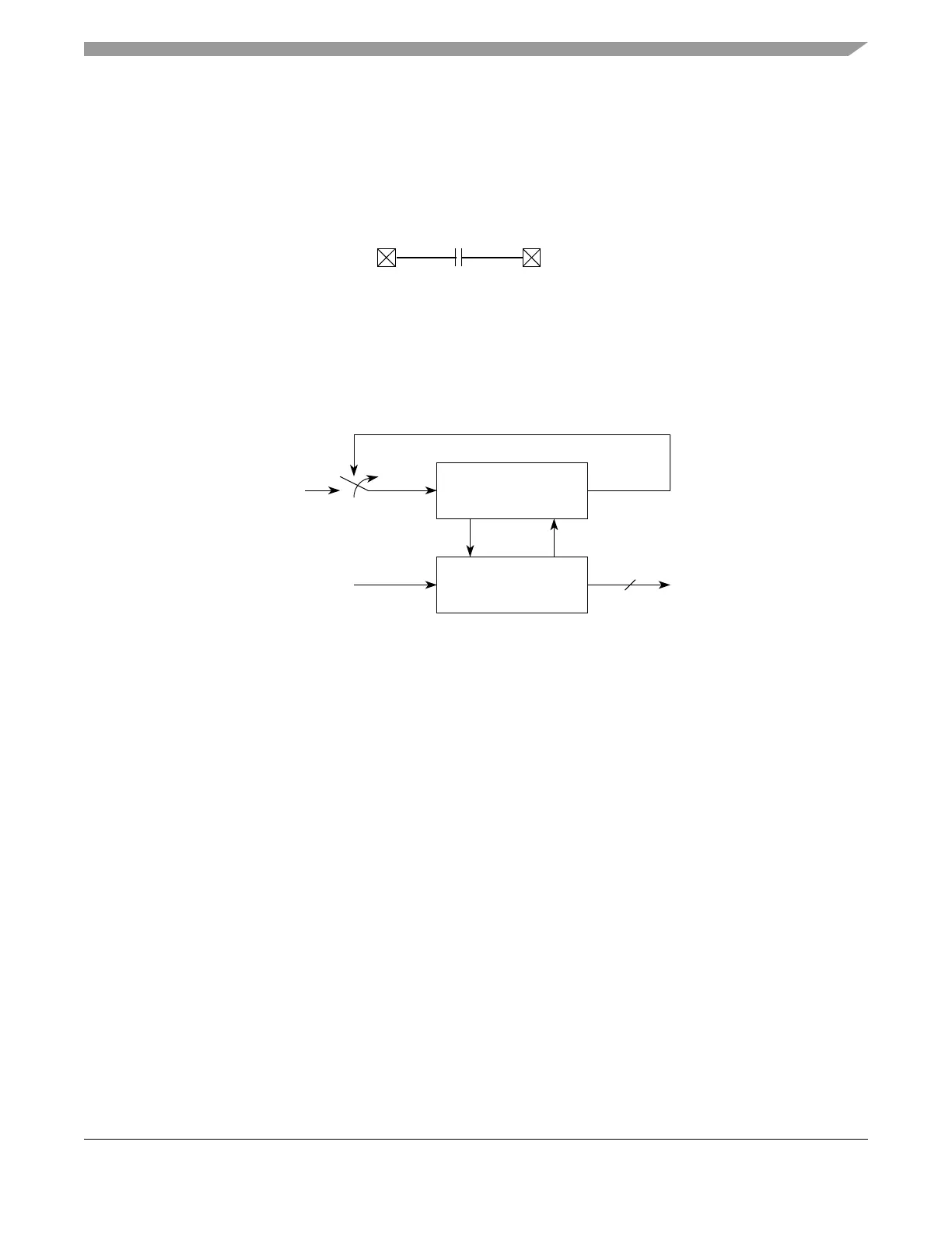
19.4.9.2 Analog-to-Digital Converter (ADC)
19.4.9.2.1 ADC Architecture
Figure 19-60. RSD ADC Block Diagram
The redundant signed digit (RSD) cyclic ADC consists of two main portions, the analog RSD stage, and
the digital control and calculation module, as shown in Figure 19-60. To begin an analog-to-digital
conversion, a differential input is passed into the analog RSD stage. The signal is passed through the RSD
stage, and then from the RSD stage output, back to its input to be passed again. To complete a 12-bit
conversion, the signal must pass through the RSD stage 12 times. Each time an input signal is read into the
RSD stage, a digital sample is taken by the digital control/calculation module. The digital
control/calculation module uses this sample to tell the analog module how to condition the signal. The
digital module also saves each successive sample and adds them according to the RSD algorithm at the
end of the entire conversion cycle.
RSD
Single-Stage
Pipeline
Sample
Digital Control
and
Calculation
pipeline_control
OutputClock
Differential
Input
12