System Interface Unit (SIU)
MPC5553/MPC5554 Microcontroller Reference Manual, Rev. 5
6-8 Freescale Semiconductor
6.3.1 Register Descriptions
The figures that describe the MPC5553/MCP5554 registers use the following notational conventions in
this section:
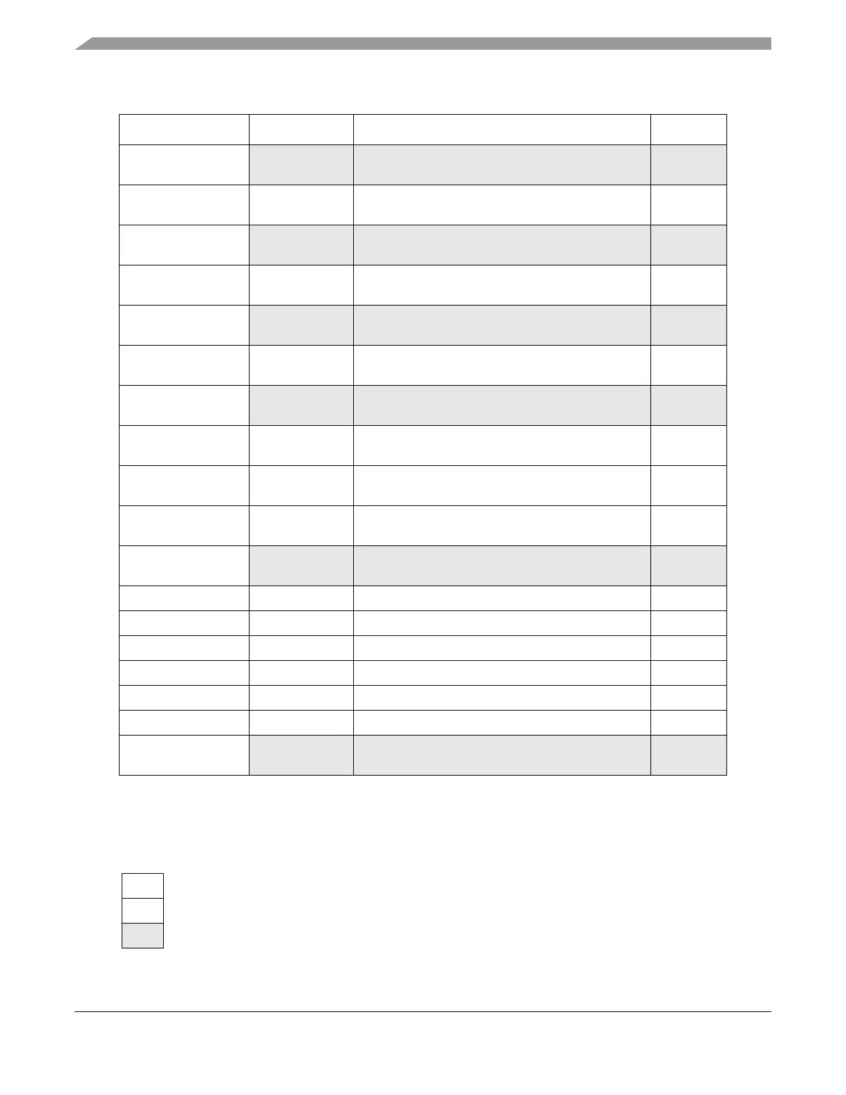
Base + 0x0034–
Base + 0x003F
— Reserved —
Base + 0x0040–
Base + 0x020C
SIU_PCR0–
SIU_PCR230
Pad configuration registers 0–230 16
Base + 0x020E–
Base + 0x05FF
— Reserved —
Base + 0x0600–
Base + 0x06D5
SIU_GPDO0–
SIU_GPDO213
GPIO pin data output registers 0–213 8
Base + 0x06D6–
Base + 0x07FF
— Reserved —
Base + 0x0800–
Base + 0x08D5
SIU_GPDI
[0:213]
GPIO pin data input registers 0–213 8
Base + 0x08D6–
Base + 0x08FF
— Reserved —
Base + 0x0900–
Base + 0x0903
SIU_ETISR eQADC trigger input select register 32
Base + 0x0904–
Base + 0x0907
SIU_EIISR External IRQ input select register 32
Base + 0x0908–
Base + 0x090B
SIU_DISR DSPI input select register 32
Base + 0x090C–
Base + 0x097F
— Reserved —
Base + 0x0980 SIU_CCR Chip configuration register 32
Base + 0x0984 SIU_ECCR External clock control register 32
Base + 0x0988 SIU_CARH Compare A high register 32
Base + 0x098C SIU_CARL Compare A low register 32
Base + 0x0990 SIU_CBRH Compare B high register 32
Base + 0x0994 SIU_CBRL Compare B low register 32
Base + 0x0998–
Base + 0x09FF
— Reserved —
w1c A write instruction of 1 clears the bit to 0.
— Not applicable.
Reserved or unimplemented bit. Do not write to this bit.
Table 6-3. SIU Address Map (Continued)
Address Register Name Register Description Bits