MPC5553/MPC5554 Microcontroller Reference Manual, Rev. 5
Freescale Semiconductor 25-33
25.11.1 Development Control Register 1, 2 (DC1, DC2)
The development control registers are used to control the basic development features of the NZ6C3
module. Development control register 1 is shown in Figure 25-13 and its fields are described in
Table 25-25.
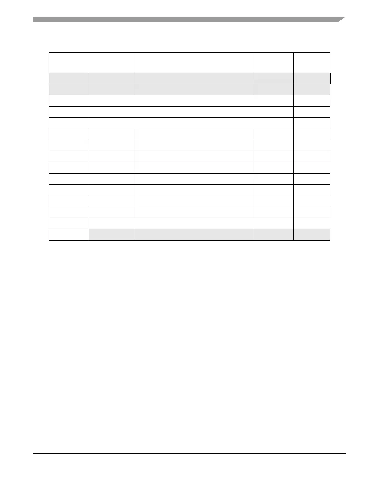
Table 25-24. NZ6C3 Memory Map
Access
Opcode
Register Name Register Description
Read
Address
Write
Address
0x1 CSC Client select control
1
1
The CSC and PCR registers are shown in this table as part of the Nexus programmer’s model. They are only
present at the top level Nexus3 controller (NPC), not in the NZ6C3 module. The device’s CSC register is
readable through Nexus3, but the PCR is shown for reference only.
0x02 —
See NPC PCR Port configuration register
1
— —
0x2 DC1 Development control 1 0x04 0x05
0x3 DC2 Development control 2 0x06 0x07
0x4 DS Development status 0x08 —
0x7 RWCS Read/write access control/status 0x0E 0x0F
0x9 RWA Read/write access address 0x12 0x13
0xA RWD Read/write access data 0x14 0x15
0xB WT Watchpoint trigger 0x16 0x17
0xD DTC Data trace control 0x1A 0x1B
0xE DTSA1 Data trace start address 1 0x1C 0x1D
0xF DTSA2 Data trace start address 2 0x1E 0x1F
0x12 DTEA1 Data trace end address 1 0x24 0x25
0x13 DTEA2 Data trace end address 2 0x26 0x27
0x14 -> 0x3F — Reserved 0x28->0x7E 0x29->0x7F