MPC5553/MPC5554 Microcontroller Reference Manual, Rev. 5
11-12 Freescale Semiconductor
NOTE
When configured for dual-controller mode, the CLKOUT clock divider on
the slave device must not be changed from its reset state of divide-by-2.
Increasing or decreasing this divide ratio will produce unpredictable results
from the FMPLL.
11.2 External Signal Description
Table 11-3 lists external signals used by the FMPLL during normal operation.
11.3 Memory Map/Register Definition
Table 11-4 shows the FMPLL memory map locations.
11.3.1 Register Descriptions
The clock operation is controlled by the synthesizer control register (FMPLL_SYNCR) and status is
reported in the synthesizer status register (FMPLL_SYNSR). The following sections describe these
registers in detail.
11.3.1.1 Synthesizer Control Register (FMPLL_SYNCR)
The synthesizer control register (FMPLL_SYNCR) contains bits for defining the clock operation for the
system.
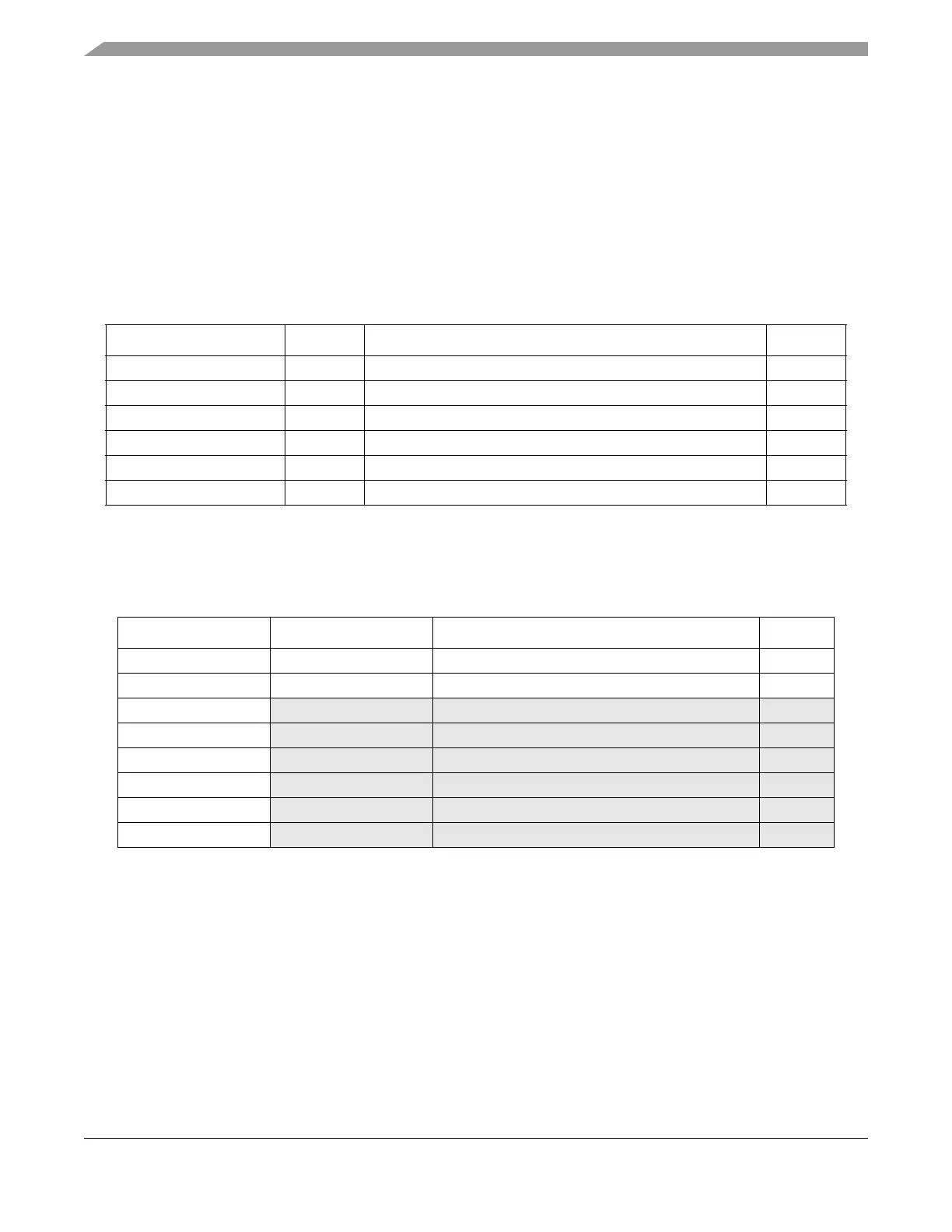
Table 11-3. PLL External Pin Interface
Name I/O Type Function Pull
PLLCFG0_GPIO208 I/O Configures the mode during reset. GPIO used otherwise. Up
PLLCFG1_GPIO209 I/O Configures the mode during reset. GPIO used otherwise. Up
XTAL Output Output drive for external crystal —
EXTAL_EXTCLK Input Crystal/external clock input —
V
DDSYN
Power Analog power supply (3.3V +/–10%) —
V
SSSYN
Ground Analog ground —
Table 11-4. FMPLL Module Memory Map
Address Register Name Register Description Size (bits)
Base (0xC3F8_0000) FMPLL_SYNCR Synthesizer control register 32
Base + 0x0004 FMPLL_SYNSR Synthesizer status register 32
Base + 0x0008
— Reserved —
Base + 0x000C — Reserved —
Base + 0x0010 — Reserved —
Base + 0x0014
— Reserved —
Base + 0x0018
— Reserved —
Base + 0x001C — Reserved —