MPC5553/MPC5554 Microcontroller Reference Manual, Rev. 5
9-2 Freescale Semiconductor
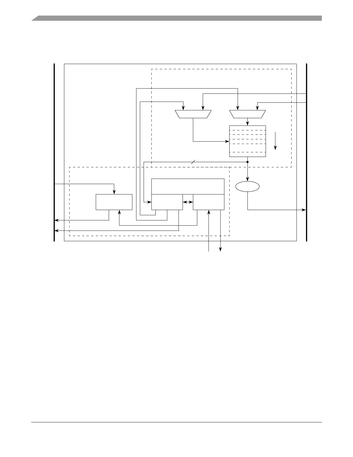
9.1.1 Block Diagram
Figure 9-1 is a block diagram of the eDMA module.
Figure 9-1. eDMA Block Diagram
9.1.2 Overview
The enhanced direct memory access (eDMA) controller hardware microarchitecture includes a DMA
engine which performs source and destination address calculations, and the actual data movement
operations, along with SRAM-based local memory containing the transfer control descriptors (TCD) for
the channels.
9.1.3 Features
The eDMA is a highly-programmable data transfer engine, which has been optimized to minimize the
required intervention from the host processor. It is intended for use in applications where the data size to
be transferred is statically known, and is not defined within the data packet itself. The eDMA module
features:
• All data movement via dual-address transfers: read from source, write to destination
— Programmable source, destination addresses, transfer size, plus support for enhanced
addressing modes
Slave Interface
eDMA
eDMA Done
System Bus
Data Path
Control
Address
Program Model/
Slave Write Data
Slave Write Address
Bus Write Data
Slave Read Data
Bus Address
eDMA Engine
TCD0
TCDn-1*
eDMA Peripheral
Bus Read Data
Channel Arbitration
Request
Path
SRAM
Transfer Control Descriptor
(TCD)
SRAM
* n = 64 channels in MPC5554
32 channels in MPC5553