MPC5553/MPC5554 Microcontroller Reference Manual, Rev. 5
Freescale Semiconductor 25-73
25.14.2 NXDM Registers
Detailed register definitions for the NXDM implementation are as follows:
25.14.2.1 Development Control Registers (DC1 and DC2)
The development control registers control the basic development features of the NXDM module.
Data Trace End Address 1 (DTEA1) 0x12 R/W 0x24 0x25
Data Trace End Address 2 (DTEA2) 0x13 R/W 0x26 0x27
Breakpoint/Watchpoint Control Register 1 (BWC1) 0x16 R/W 0x2C 0x2D
Breakpoint/Watchpoint Control Register 2 (BWC2) 0x17 R/W 0x2E 0x2F
Breakpoint/Watchpoint Address Register 1 (BWA1) 0x1E R/W 0x3C 0x3D
Breakpoint/Watchpoint Address Register 2 (BWA2) 0x1F R/W 0x3E 0x3F
Reserved 0x20–0x3F – 0x40–0x7E 0x41–0x7F
1
The CSC and PCR registers are shown in this table as part of the Nexus programmer’s model. They are only present
at the top level Nexus3 controller (NPC), not in the NXDM module. The device’s CSC register is readable through
Nexus3; the PCR is shown for reference only.
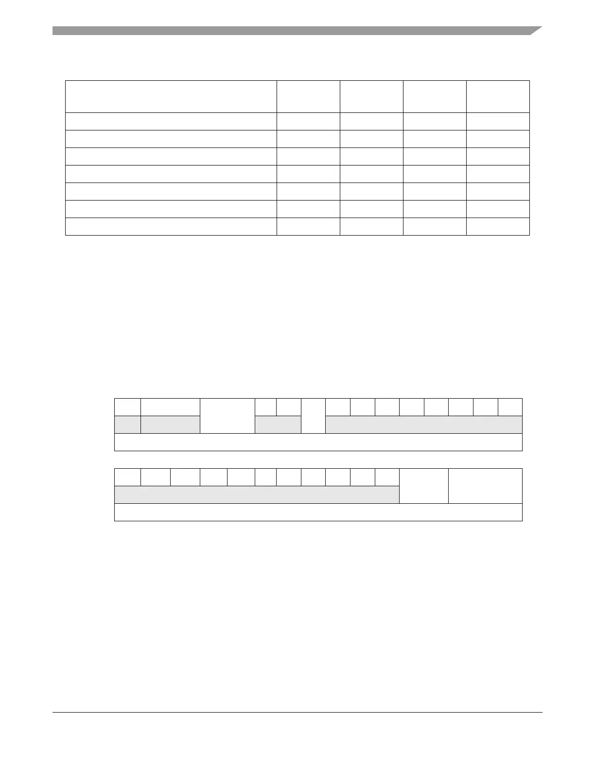
31 30 29 28 27 26 25 24 23 22 21 20 19 18 17 16
ROPCMCK_DIV EOC 00WEN00000000
W
Reset0 0 0 0 000000000000
1514131211109876543210
R0 0 0 0 0000000 EIC TM
W
Reset0 0 0 0 000000000000
Figure 25-53. Development Control Register 1 (DC1)
Table 25-45. NXDM Register Map (Continued)
Nexus Register
Nexus Access
Opcode
Read/Write
Read
Address
Write
Address