MPC5553/MPC5554 Microcontroller Reference Manual, Rev. 5
Freescale Semiconductor 21-3
21.2 External Signal Description
This section provides a description of all module signals external to the MCU.
21.2.1 Overview
Each eSCI module has two I/O signals connected to the external MCU pins. These signals are summarized
in Table 21-1 and described in more detail in the following sections.
21.2.2 Detailed Signal Description
21.2.2.1 SCI Transmit (TXDx)
This pin serves as transmit data output of eSCI.
21.2.2.2 SCI Receive Pin (RXDx)
This pin serves as receive data input of the eSCI.
21.3 Memory Map/Register Definition
21.3.1 Overview
This section provides a detailed description of all memory and registers.
21.3.2 Module Memory Map
The memory map for the eSCI module is given below in Table 21-2. The address offset is listed for each
register. The total address for each register is the sum of the base address for the eSCI module
(ESCIx_base) and the address offset for each register. There are two eSCI modules on the
MPC5553/MPC5554: the base is 0xFFFB_0000 for eSCIA and 0xFFFB_4000 for eSCIB.
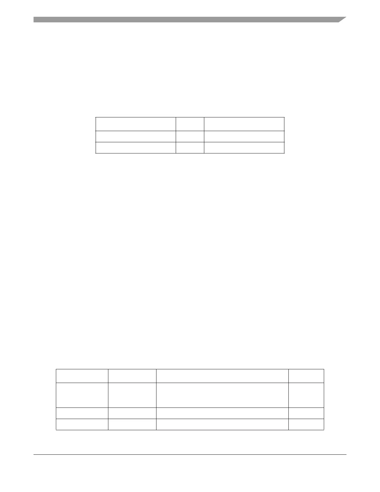
Table 21-1. eSCI Signals
Signal Name
1
1
x indicates eSCI module A or B
I/O Description
RXDx I eSCI Receive
TXDx OeSCI Transmit
Table 21-2. Module Memory Map
Address Register Name Register Description Size (bits)
Base
0xFFFB_0000 (A)
0xFFFB_4000 (B)
ESCIx_CR1 eSCI control register 1 32
Base + 0x0004 ESCIx_CR2 eSCI control register 2 16
Base + 0x0006 ESCIx_DR eSCI data register 16