MPC5553/MPC5554 Microcontroller Reference Manual, Rev. 5
21-4 Freescale Semiconductor
21.3.3 Register Definition
This section consists of register descriptions in address order. Each description includes a standard register
diagram with an associated figure number. Details of register bit and field function follow the register
diagrams, in bit order.
21.3.3.1 eSCI Control Register 1 (ESCIx_CR1)
Base + 0x0008 ESCIx_SR eSCI status register 32
Base + 0x000C ESCIx_LCR LIN control register 32
Base + 0x0010 ESCIx_LTR LIN transmit register 32
Base + 0x0014 ESCIx_LRR LIN receive register 32
Base + 0x0018 ESCIx_LPR LIN cyclic redundancy check polynomial register 32
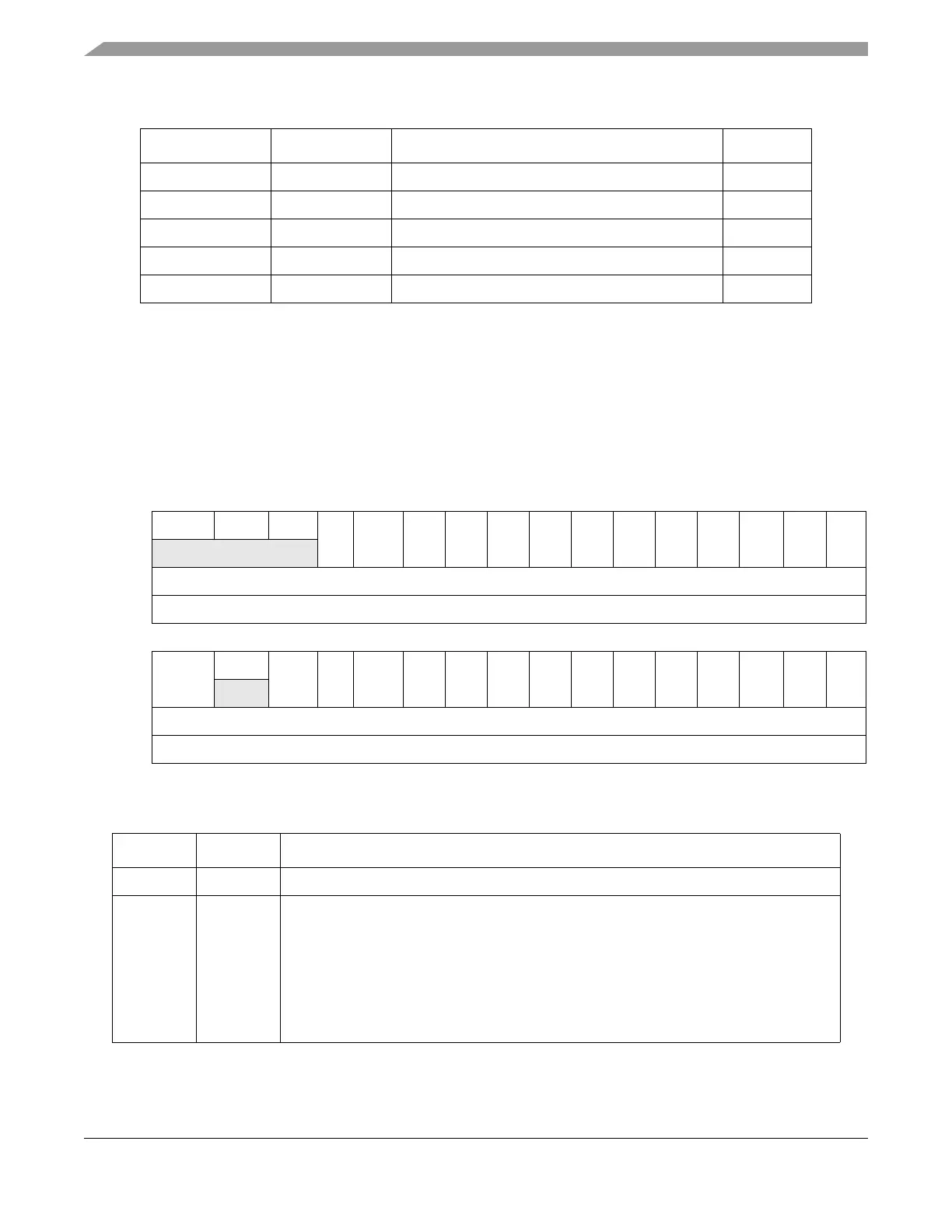
0 1 234 56789101112131415
R 0 0 0 SBR
0
SBR
1
SBR
2
SBR
3
SBR
4
SBR
5
SBR
6
SBR
7
SBR
8
SBR
9
SBR
10
SBR
11
SBR
12
W
Reset0 0 000 00000000100
Reg Addr Base + 0x0000
16 17 18 19 20 21 22 23 24 25 26 27 28 29 30 31
R LOOPS 0 RSRC M WAKE ILT PE PT TIE TCIE RIE ILIE TE RE RWU SBK
W
Reset0 0 000 00000000000
Reg Addr Base + 0x0000
Figure 21-2. eSCI Control Register 1 (ESCIx_CR1)
Table 21-3. ESCIx_CR1 Field Descriptions
Bits Name Description
0–2 — Reserved.
3–15 SBRn SCI baud rate. Used by the counter to determine the baud rate of the eSCI. The formula
for calculating the baud rate is:
where BR is the content of the eSCI control register 1 (ESCIx_CR1), bits SBR0–SBR12.
SBR0–SBR12 can contain a value from 1 to 8191.
Also refer to the ESCIx_LCR[WU] bit description on page 21-13.
Table 21-2. Module Memory Map (Continued)
Address Register Name Register Description Size (bits)
SCI baud rate
eSCI system clock
16 BR
-------------------------------------------------=