MPC5553/MPC5554 Microcontroller Reference Manual, Rev. 5
Freescale Semiconductor 12-7
12.2.1 Detailed Signal Descriptions
The MPC5554 and the 416 and 324 BGA packages of the MPC5553 have pinned out EBI signals. The 208
BGA package of the MPC5553 does not pin out these signals.
12.2.1.1 Address Lines 8–31 (ADDR[8:31])
The ADDR[8:31] signals specify the physical address of the bus transaction. Both the MPC5554 and the
416 BGA of the MPC5553 have 24 bits available as external pins.
The 24 address lines correspond to bits 8–31 of the EBI’s 32-bit internal address bus. Bits 0–7 are
internally driven by the EBI for externally initiated accesses depending on which internal slave is to be
accessed. See Section 12.4.2.10.1, “Address Decoding for External Master Accesses,” for more details.
ADDR[8:31] is driven by the EBI or an external master depending on who owns the external bus.
Note that the 324 package of the MPC5553 uses only ADDR[12:31], but if CS[0:3] are configured to
ADDR[8:11] then the full 24 address lines are available.
The calibration bus shares ADDR[12:26] with the EBI’s primary bus.
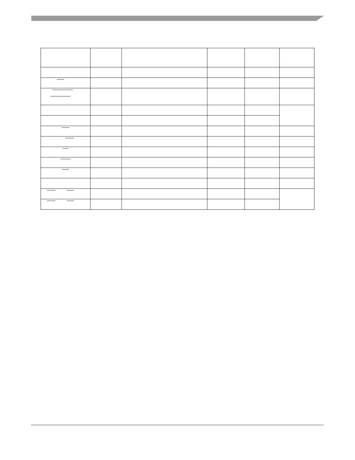
CLKOUT
3
Output Clockout Enabled 416, 324 Yes
CS[0:3] Output Chip Selects Up 416, 324 Yes
CAL_CS[0]
CAL_CS[2:3]
Output Calibration Chip Selects Up 416, 324 No
DATA[0:15] I/O Data Bus — 416, 324
Ye s
DATA[16:31]
2
I/O Data Bus — 416
OE Output Output Enable Up 416, 324 Yes
RD_WR
2
I/O Read_Write Up 416, 324 Yes
TA I/O Transfer Acknowledge Up 416, 324 Yes
TEA I/O Transfer Error Acknowledge Up 416 Yes
TS I/O Transfer Start Up 416, 324 Yes
TSIZ[0:1] I/O Transfer Size — None Yes
WE[0:1]/BE[0:1] Output Write/Byte Enables Up 416, 324
Ye s
WE[2:3]/BE[2:3] Output Write/Byte Enables Up 416
1
This column shows which signals require a weak pull-up or pull-down. The EBI module does not contain these
pull-up/pull-down devices within the module, but instead are controlled by the pad configuration registers in the System
Integration Module (SIU_PCRs).
2
These signals are also used by the calibration bus of the MPC5553.
3
The CLKOUT signal is driven by the FMPLL Module.
Table 12-3. Signal Properties (Continued)
Name I/O Type Function Pull
1
MPC5553
Packages
MPC5554
Package