MPC5553/MPC5554 Microcontroller Reference Manual, Rev. 5
Freescale Semiconductor 13-1
Chapter 13
Flash Memory
13.1 Introduction
This section provides information about the flash bus interface unit (FBIU) and the flash memory block of
the MPC5553/MPC5554.
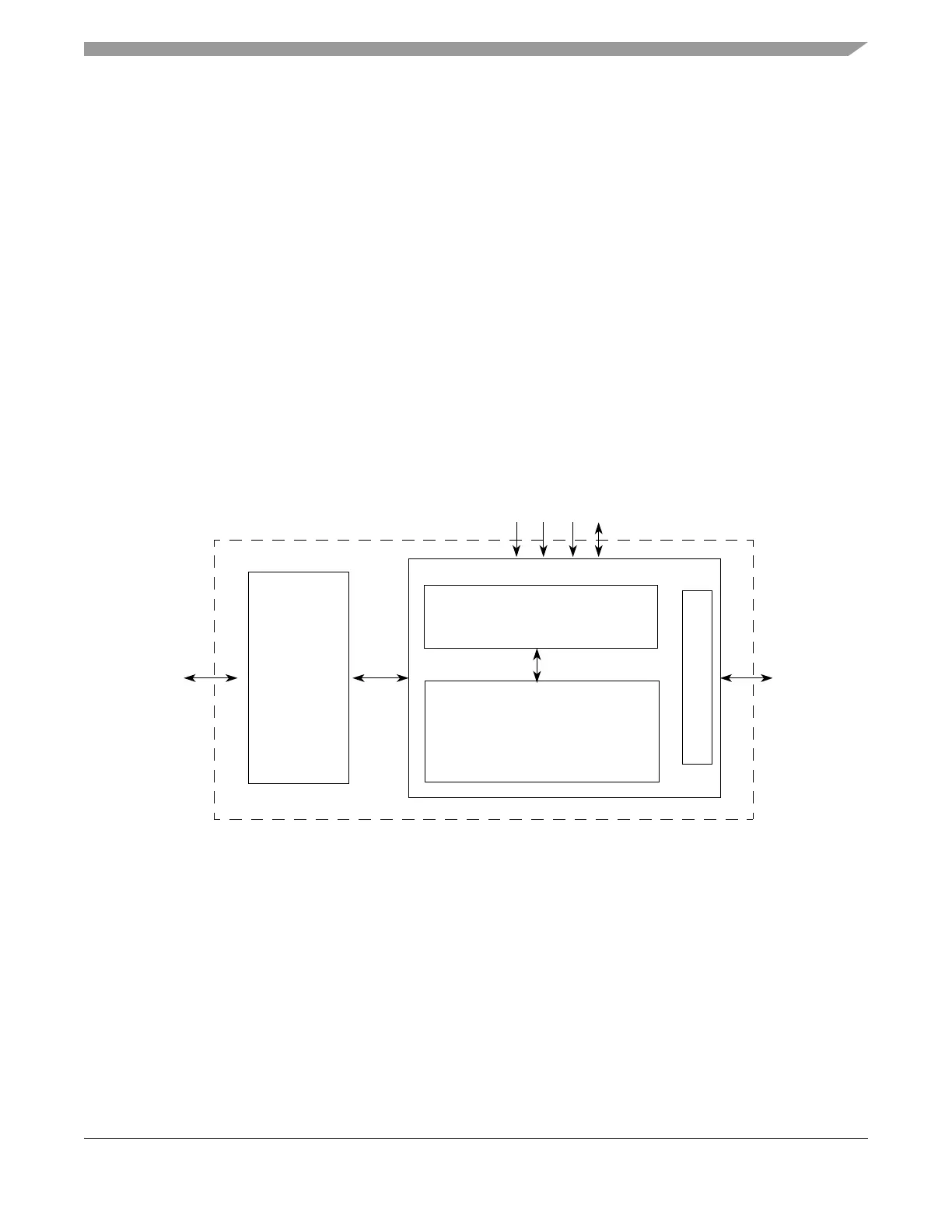
13.1.1 Block Diagram
Figure 13-1 shows a block diagram of the flash memory module. The FBIU is addressed through the
system bus while the flash control and status registers are addressed through the slave (peripheral) bus.
Figure 13-1. Flash System Block Diagram
13.1.2 Overview
The flash module serves as electrically programmable and erasable non-volatile memory (NVM) that is
ideal for program and data storage for single-chip applications allowing for field reprogramming without
requiring external programming voltage sources. The module is a solid-state silicon memory device
consisting of blocks of single-transistor storage elements.
The MPC5553/MPC5554 flash contains a flash bus interface unit (FBIU) and a flash memory array. The
FBIU interfaces the system bus to a dedicated flash memory array controller. The FBIU supports a 64-bit
data bus width at the system bus port, and a 256-bit read data interface from the flash memory array. If
enabled, the FBIU contains a two-entry prefetch buffer, each entry containing 256 bits of data, and an
Flash Memory Interface (MI)
Flash Core
System
V
DD
Vssf
V
FLASH
V
PP
Flash Memory Block
Flash Bus
(FBIU)
Control/Status Registers
Slave Bus
Bus
Interface
Unit