MPC5553/MPC5554 Microcontroller Reference Manual, Rev. 5
Freescale Semiconductor 2-5
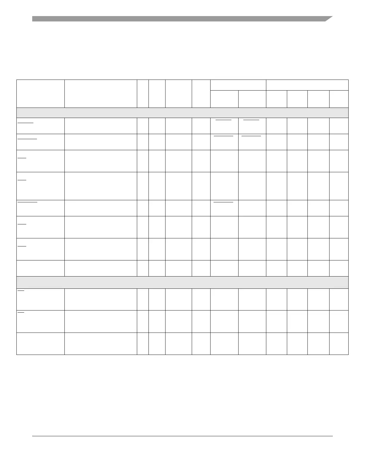
2.2.1 MPC5553 Signals Summary
Table 2-1 gives a summary of the MPC5553 external signals and properties.
Table 2-1. MPC5553 Signal Properties
Signal Name
1
Signal Functions
2
P/
A/G
I/O
Type
Voltage
3
Pad
Type
4
Status Pin Labels / Package Type
During
Reset
5
After
Reset
6
496
7
416
8
324 208
9
Reset / Configuration Signals
RESET
External Reset Input P I V
DDEH6
S
RESET
/
Up
RESET /
Up
AA27 W26 R22 L16
RSTOUT
External Reset Output P O V
DDEH6
S
RSTOUT
/
Low
RSTOUT /
High
W26 V25 P21 K15
PLLCFG[0]_
IRQ
[4]_
GPIO[208]
FMPLL Mode Selection
External Interrupt Request
General Purpose I/O
P
A
G
I
I
I/O
V
DDEH6
M
PLLCFG /
Up
– / Up AB27 AB25 V21 M14
PLLCFG[1]_
IRQ
[5]_
SOUTD_
GPIO[209]
FMPLL Mode Selection
External Interrupt Request
DSPI D Data Output
General Purpose I/O
P
A
A2
G
I
I
O
I/O
V
DDEH6
M
PLLCFG /
Up
– / Up AA26 AA24 U20 N15
RSTCFG
_
GPIO[210]
Reset Configuration Input
General Purpose I/O
P
G
I
I/O
V
DDEH6
S
RSTCFG
/
Up
– / Up Y28 V26 P22 —
BOOTCFG[0]_
10
IRQ[2]_
GPIO[211]
Boot Configuration Input
External Interrupt Request
General Purpose I/O
P
A
G
I
I
I/O
V
DDEH6
S
BOOTCFG /
Down
– / Down AB26 AA25 U21 —
BOOTCFG[1]_
IRQ
[3]_
GPIO[212]
Boot Configuration Input
External Interrupt Request
General Purpose I/O
P
A
G
I
I
I/O
V
DDEH6
S
BOOTCFG /
Down
– / Down AB24 Y24 T20 M15
WKPCFG_
GPIO[213]
Weak Pull Configuration Input
General Purpose I/O
P
G
I
I/O
V
DDEH6
S
WKPCFG /
Up
– / Up AA24 Y23 R19 L15
External Bus Interface (EBI)
11
and Calibration Bus Interface (CBI)
12
Signals
CS[0]_
ADDR[8]_
13
GPIO[0]
External Chip Select 0
External Address Bus
13, 14
General Purpose I/O
P
A
G
O
I/O
I/O
V
DDE2
F – / Up – / Up
15
T7 P4 M4 R1
CS
[1:3]_
ADDR[9:11]_
13
GPIO[1:3]
External Chip Selects 1–3
External Address Bus
13, 14
General Purpose I/O
P
A
G
O
I/O
I/O
V
DDE2
F – / Up – / Up
15
R5, P5,
R7
P3, P2,
P1
M3, N2,
N1
—
ADDR[8:11]_
13
CAL_ADDR[27:30]_
GPIO[4:7]
External Address Bus
13, 14
Calibration Address Bus
General Purpose I/O
P
A
G
I/O
O
I/O
V
DDE2
F – / Up – / Up
15
Y5, Y3,
AA3,
AB3
V4,
W3:4,
Y3
——