MPC5553/MPC5554 Microcontroller Reference Manual, Rev. 5
23-2 Freescale Semiconductor
23.2.1 Detailed Signal Description
The following paragraphs provide descriptions of signals coming into and going out of the VRC.
23.2.1.1 V
RC33
3.3 V VRC supply input.
23.2.1.2 V
DDSYN
3.3 V supply input for FMPLL.
23.2.1.3 V
DDEH6
Power supply input for padring segment that contains the RESET pad.
23.2.1.4 V
RCVSS
3.3 V VRC ground supply.
23.2.1.5 V
RCSNS
1.5 V sense from external 1.5 V supply output of NPN transistor. This input is monitored by the VRC to
determine current value for V
RCCTL
. VRCSNS is a pad on the die that is connected to a V
DD
plane inside
the package. It is not a package ball.
23.2.1.6 V
RCCTL
The V
RCCTL
sources base current to the external bypass transistor. The V
RCCTL
signal is used with internal
and external transistors to provide V
DD
, which is the MCU’s 1.5V power supply.
23.2.1.7 V
DD
Internal 1.5 V supply input.
23.3 Memory Map/Register Definition
The VRC and POR module has no memory-mapped registers.
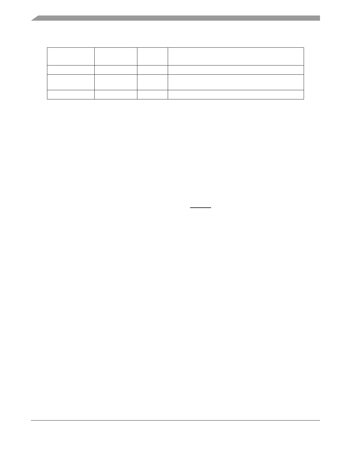
V
RCVSS
Supply pin 0 V Regulator supply ground
VRCSNS 1.5-V Sense 1.5 V 1.5-V Sense used by VRC. Pad connected to V
DD
plane in
package—not a package ball.
V
RCCTL
Current output — Regulator control output
Table 23-1. Voltage Regulator Controller and POR Block External Signals (Continued)
Signal Type
Signal
Level
Description