MPC5553/MPC5554 Microcontroller Reference Manual, Rev. 5
17-2 Freescale Semiconductor
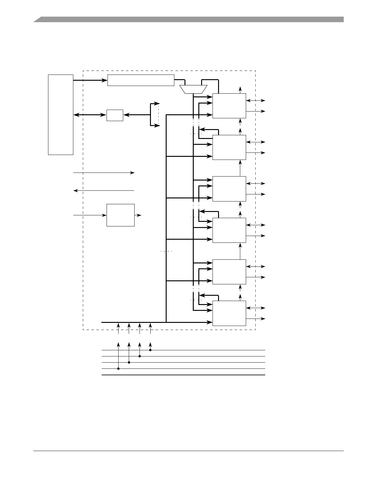
17.1.1 Block Diagram
Figure 17-1 shows the block diagram of the eMIOS.
Figure 17-1. eMIOS Block Diagram
See Note 1
[D][A]
Counter
Buses
(Time
Bases)
EMIOS16
EMIOS_Flag_Out16
[C][A]
[B][A]
•
•
•
•
•
•
Counter
Buses
(Time
Bases)
Counter
Buses
(Time
Bases)
All
Submodules
Internal
Counter
Clock
Enable
STAC
Output Disable Input[0:3]
Global Time
Base Enable In
Global Time
Base Enable Out
System
Clock
Enhanced Modular
Unified
STAC Client Submodule
BIU
Slave
Interface
Clock
Prescaler
Output Disable
Control Bus
Note 1: Connection between UC[n-1] and UCn necessary to implement QDEC mode.
Input/Output
•
•
•
•
•
•
•
•
•
•
•
•
Subsystem
Channel
23
EMIOS23
EMIOS_Flag_Out23
Unified
Channel
16
Unified
Channel
15
EMIOS15
EMIOS_Flag_Out15
Unified
Channel
8
Unified
Channel
7
Unified
Channel
0
EMIOS8
EMIOS_Flag_Out8
EMIOS7
EMIOS_Flag_Out7
EMIOS0
EMIOS_Flag_Out0
EMIOS_Flag_Out8
EMIOS_Flag_Out9
EMIOS_Flag_Out10
EMIOS_Flag_Out11
EMIOS_Flag_Out[20:23]
ETPUA_ODI3
ETPUA_ODI2
ETPUA_ODI1
ETPUA_ODI0
ETPUB_ODI[0:3]
Internal
Bus
Note 2: On channels 12–15, there is no input from EMIOS[12:15], but only from the DSPI module.
See Note 2