MPC5553/MPC5554 Microcontroller Reference Manual, Rev. 5
10-8 Freescale Semiconductor
10.3 Memory Map/Register Definition
Table 10-2 is the INTC memory map. INTC_BASE for the MPC5553/MPC5554 is located at
0xFFF4_8000.
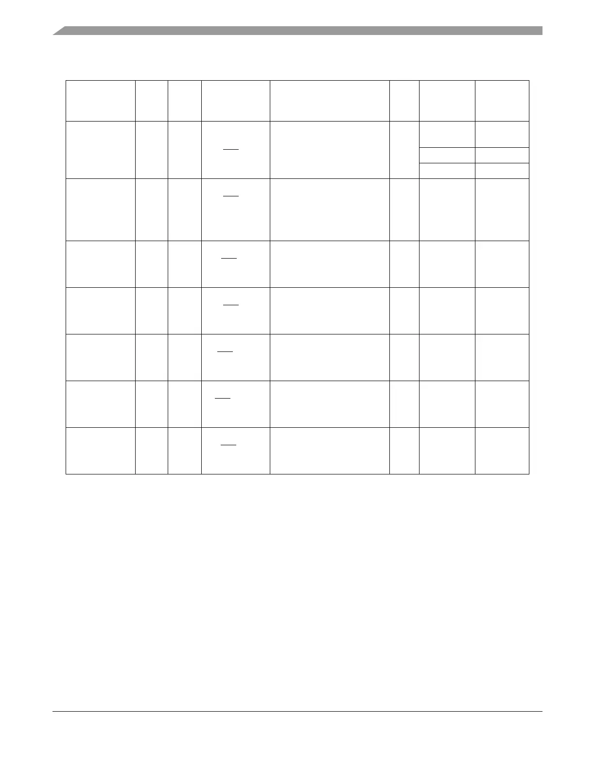
PLLCFG[0] AB25 P PLLCFG[0] FMPLL mode selection I PLLCFG /
Up
— / Up
AIRQ[4] External Interrupt Request I
G GPIO[208] GPIO I/O
PLLCFG[1] AA24 P PLLCFG[1] FMPLL mode selection I PLLCFG /
Up
— / Up
AIRQ
[5] External Interrupt Request I
A2 SOUTD DSPI D Data Output O
G GPIO[209] GPIO I/O
TCRCLKB
6
M23 P TCRCLKB eTPU B TCR clock I — / Up — / Up
AIRQ[6]
6
External Interrupt Request
6
I
G GPIO[146] GPIO I/O
TCRCLKA N4 P TCRCLKA eTPU A TCR clock I — / Up — / Up
AIRQ
[7] External interrupt request I
G GPIO[113] GPIO I/O
ETPUA[20:23] H1:G4
G2:G1
P ETPUA[20:23] eTPU A channel I/O — /
WKPCFG
— /
WKPCFG
AIRQ
[8:11] External interrupt request I
G GPIO[134:137] GPIO I/O
ETPUA[24:26] F1:G3:
F3
P ETPUA[24:26] eTPU A channel (output only) O —
/WKPCFG
—
/WKPCFG
AIRQ
[12:14] External interrupt request I
G GPIO[138:140] GPIO I/O
ETPUA27 F2 P ETPUA[27] eTPU A channel (output only) O —
/WKPCFG
—
/WKPCFG
AIRQ
[15] External interrupt request I
G GPIO[141] GPIO I/O
1
This is the name that appears on the PBGA pinout.
2
Primary, alternate, or GPIO function.
3
For each pin in the table, each line in the function column is a separate function of the pin. For all MPC5554/MPC5553
I/O pins the selection of primary, secondary or tertiary function is done in the MPC5554/MPC5553 SIU except where
explicitly noted.
4
Terminology is O - output, I - input, Up - weak pullup enabled, Down - weak pulldown enabled, Low - output driven low,
High - output driven high.
5
Function after reset of GPI is general-purpose input.
6
This signal appears only in the MPC5554, it is not implemented in the MPC5553.
Table 10-1. External Interrupt Signals (Continued)
Signal
1
Pin P/A/G
2
Function
3
Description
I/O
Type
Reset
Function/
State
4
Post Reset
Function/
State
5