MPC5553/MPC5554 Microcontroller Reference Manual, Rev. 5
Freescale Semiconductor 20-5
PCS0/SS must be configured as input and pulled high. If the internal pull up is being used then the
appropriate bits in the relevant SIU_PCR must be set (SIU_PCR [WPE=1], [WPS=1]). For more
information, see Section 20.4.1.2, “Slave Mode.”
20.1.4.3 Module Disable Mode
The module disable mode is used for MCU power management. The clock to the non-memory mapped
logic in the DSPI is stopped while in module disable mode. The DSPI enters the module disable mode
when the MDIS bit in DSPIx_MCR is set. For more information, see Section 20.4.1.3, “Module Disable
Mode.”
20.1.4.4 Debug Mode
Debug mode is used for system development and debugging. If the device enters debug mode while the
FRZ bit in the DSPIx_MCR is set, the DSPI halts operation on the next frame boundary. If the device enters
debug mode while the FRZ bit is negated, the DSPI behavior is unaffected and remains dictated by the
module-specific mode and configuration of the DSPI. For more information, see Section 20.4.1.4, “Debug
Mode.”
20.2 External Signal Description
20.2.1 Signal Overview
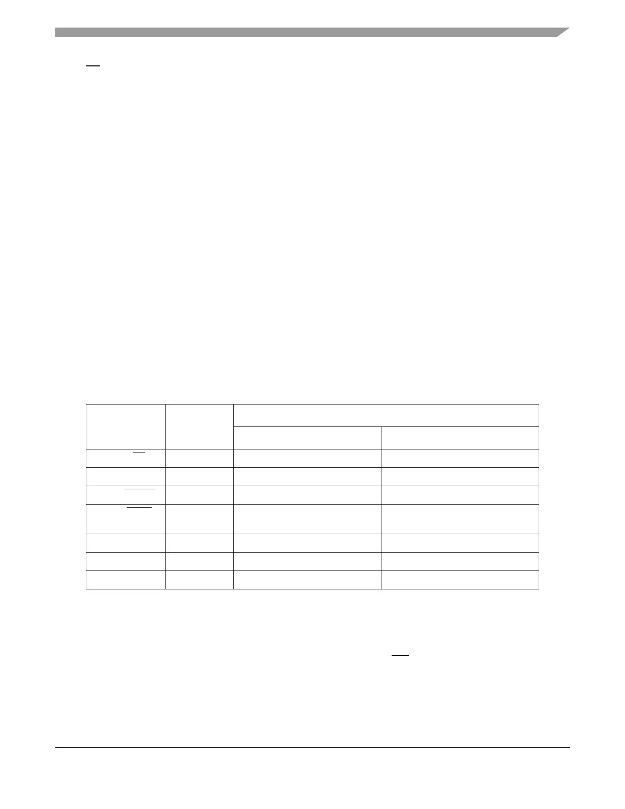
Table 20-1 lists off-chip DSPI signals.
20.2.2 Signal Names and Descriptions
20.2.2.1 Peripheral Chip Select / Slave Select (PCS0/SS)
In master mode, the PCS0 signal is a peripheral chip select output that selects the slave device to which
the current transmission is intended.
Table 20-1. Signal Properties
Name I/O Type
Function
Master Mode Slave Mode
PCS0/SS
Output / Input Peripheral chip select 0 Slave select
PCS[1:3] Output Peripheral chip select 1–3 Unused
1
1
In the SIU the user can select alternate pin functions for the MPC5553/MPC5554.
PCS4/MTRIG
Output Peripheral chip select 4 Master Trigger
PCS5/PCSS
Output Peripheral chip select 5 /
Peripheral chip select strobe
Unused
1
SIN Input Serial data in Serial data in
SOUT Output Serial data out Serial data out
SCK Output / Input Serial clock (output) Serial clock (input)