MPC5553/MPC5554 Microcontroller Reference Manual, Rev. 5
2-8 Freescale Semiconductor
RD_WR_
18
GPIO[62]
External Data Bus Read/Write
General Purpose I/O
P
G
I/O
I/O
V
DDE2
F – / Up – / Up
15
U3 T3 P3 —
BDIP
_
GPIO[63]
External Burst Data In Progress
General Purpose I/O
P
G
O
I/O
V
DDE2
F – / Up – / Up
15
N1 N1 M1 —
WE
/BE[0:1]_
19
GPIO[64:65]
External Write/Byte Enable
19
General Purpose I/O
P
G
O
I/O
V
DDE2
F – / Up – / Up
15
U5, T5 R4, R3 N3:4 —
WE
/BE[2:3]_
19
CAL_WE/BE[0:1]_
19
GPIO[66:67]
External Write/Byte Enable
19
Calibration Write/Byte Enable
19
General Purpose I/O
P
A
G
O
O
I/O
V
DDE2
F – / Up – / Up
15
N3, P1 R1:2 — —
OE
_
20
GPIO[68]
External Bus Output Enable
General Purpose I/O
P
G
O
I/O
V
DDE3
17
F – / Up – / Up
15
AF16 AE12 AB9 T3
TS
_
21
GPIO[69]
External Bus Transfer Start
General Purpose I/O
P
G
I/O
I/O
V
DDE2
F – / Up – / Up
15
W3 V3 T4 —
TA
_
GPIO[70]
External Transfer Acknowledge
General Purpose I/O
P
G
I/O
I/O
V
DDE2
F – / Up – / Up
15
V3 U3 R4 —
TEA
_
CAL_CS
[0]_
GPIO[71]
External Transfer Error Acknowledge
Calibration Chip Select
General Purpose I/O
P
A
G
I/O
O
I/O
V
DDE2
F – / Up – / Up
15
N2 N2 — —
BR
_
22
CAL_ADDR[10]_
FEC_MDC_
CAL_CS
[2]_
GPIO[72]
—
Calibration Address Bus
FEC Management Clock
Calibration Chip Select
General Purpose I/O
—
MP
A
A2
G
—
I/O
O
O
I/O
V
DDE3
17
F – / Up – / Up
15
AF17 AE13 — —
BG
_
22
CAL_ADDR[11]_
FEC_MDIO_
CAL_CS
[3]_
GPIO[73]
—
Calibration Address Bus
FEC Management Data I/O
Calibration Chip Select
General Purpose I/O
—
MP
A
A2
G
—
I/O
I/O
O
I/O
V
DDE3
17
F — / Up — / Up
15
AG16 AE14 — —
Nexus Signals
EVTI Nexus Event In P I V
DDE7
F I / Up EVTI / Up G26 F25 F21 E15
EVTO
Nexus Event Out P O V
DDE7
F O / Low EVTO / High G27 F26 F22 D15
MCKO Nexus Message Clock Out P O V
DDE7
F O / Low
MCKO /
Enabled
23
H26G24G20F15
MDO[0]
24
Nexus Message Data Out P O V
DDE7
F O / High MDO / Low C25 B24 B20 A14
MDO[3:1] Nexus Message Data Out P O V
DDE7
F O / Low MDO / Low
C23,
B21,
C24
C22,
D21,
C23
D18,
C18:19
B13,
A13,
B14
MDO[11:4]_
25
GPIO[82:75]
Nexus Message Data Out
General Purpose I/O
P
G
O
I/O
V
DDE7
F O / Low – / Down
A23,
C22,
A20,
A24,
B23,
B20,
C20,
B24
A22,
B21,
C20,
A23,
B22,
C21,
D20,
B23
A17:18,
B17,
A19,
B18,
D17,
C17, B19
—
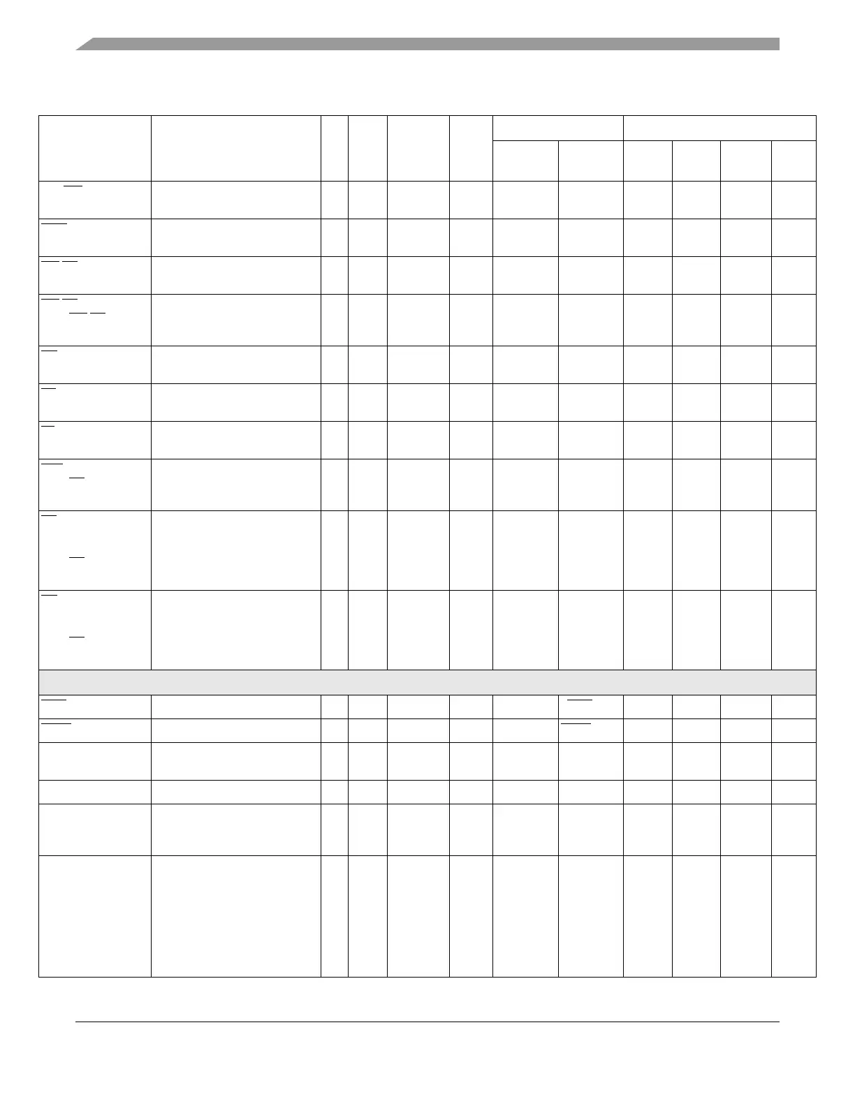
Table 2-1. MPC5553 Signal Properties (Continued)
Signal Name
1
Signal Functions
2
P/
A/G
I/O
Type
Voltage
3
Pad
Type
4
Status Pin Labels / Package Type
During
Reset
5
After
Reset
6
496
7
416
8
324 208
9