MPC5553/MPC5554 Microcontroller Reference Manual, Rev. 5
Freescale Semiconductor 2-23
ADDR[8:31]_
9
,
11
GPIO[4:27]
External Address Bus
9
, 11
General Purpose I/O
P
G
I/O
I/O
V
DDE2
F – / Up – / Up
10
Y5, Y3,
AA3, AB3,
Y7, AC3,
AC5, AB5,
T3, T2, T1,
V2, W1:2,
Y1:2, AA2,
AB2, AC2,
AD2, AD3,
AD1, AF2,
AE3
V4, W3,
W4, Y3,
AA4, AA3,
AB4, AB3,
U1, V2,
V1, W2,
W1, Y2,
Y1, AA2,
AA1, AB2,
AC1, AC2,
AD1, AE1,
AD2, AC3
DATA[0:31]_
GPIO[28:59]
External Data Bus
11
General Purpose I/O
P
G
I/O
I/O
V
DDE3
17
F – / Up – / Up
10
G11, AF12,
AG13,
AH13,
AG14,
AH15,
AG15,
AH16,
AB12,
AF10,
AD13,
AF11,
AB15,
AD12,
AD15,
AF13, AF5,
AG5, AH5,
AG6:9,
AH9, AD7,
AF6, AB9,
AF7, AD8,
AF8,
AD10:11
AE8, AF9,
AE9, AF10,
AE10,
AF12,
AE11,
AF13,
AC11,
AD11,
AC12,
AD12,
AC14,
AD13,
AC15,
AD14,
AF3, AE4,
AF4, AE5,
AF6, AE6,
AF7, AE7,
AD5, AD6,
AC6, AD7,
AC7, AD8,
AC9, AC10
TSIZ[0:1]_
GPIO[60:61]
External Transfer Size
General Purpose I/O
P
G
I/O
I/O
V
DDE2
F – / Up – / Up
10
R2, P2 T2, U2
RD_WR
_
GPIO[62]
External Read/Write
General Purpose I/O
P
G
I/O
I/O
V
DDE2
F – / Up – / Up
10
U3 T3
BDIP
_
GPIO[63]
External Burst Data In Progress
General Purpose I/O
P
G
O
I/O
V
DDE2
F – / Up – / Up
10
N1 N1
WE
/BE[0:3]_
12
GPIO[64:67]
External Write/Byte Enable
General Purpose I/O
P
G
O
I/O
V
DDE2
F – / Up – / Up
10
U5, T5, N3,
P1
R4, R3,
R2, R1
OE
_
GPIO[68]
External Output Enable
General Purpose I/O
P
G
O
I/O
V
DDE3
17
F – / Up – / Up
10
AF16 AE12
TS
_
GPIO[69]
External Transfer Start
General Purpose I/O
P
G
I/O
I/O
V
DDE2
F – / Up – / Up
10
W3 V3
TA
_
GPIO[70]
External Transfer Acknowledge
General Purpose I/O
P
G
I/O
I/O
V
DDE2
F – / Up – / Up
10
V3 U3
TEA
_
GPIO[71]
External Transfer Error Acknowledge
General Purpose I/O
P
G
I/O
I/O
V
DDE2
F – / Up – / Up
10
N2 N2
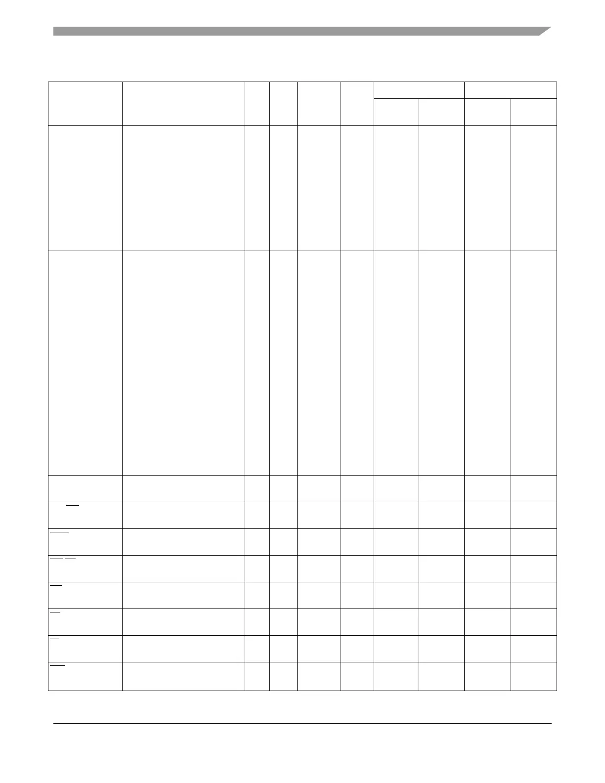
Table 2-2. MPC5554 Signal Properties (Continued)
Signal Names
1
Signal Functions
2
P/
A/
G
I/O
Type
Voltage
3
Pad
Type
4
Status Pin Labels / Package
During
Reset
5
After
Reset
6
496
7
416