MPC5553/MPC5554 Microcontroller Reference Manual, Rev. 5
21-38 Freescale Semiconductor
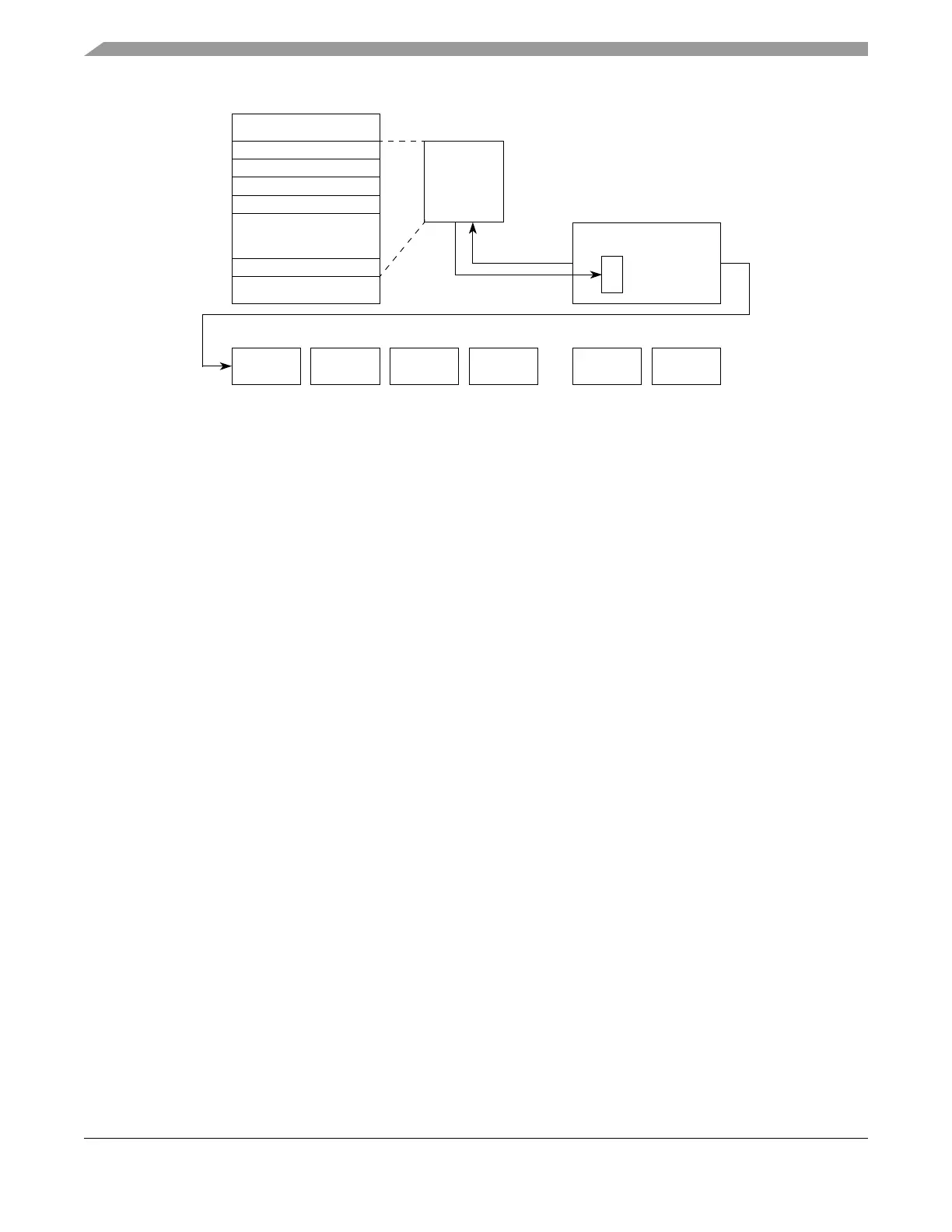
Figure 21-25. DMA Transfer of a TX frame
21.4.10.3 Generating an RX Frame
For RX frames the header information is provided by the LIN master. The data, CRC and checksum bytes
(as enabled) are provided by the LIN slave. The LIN master verifies CRC and checksum bytes transmitted
by the slave.
For a RX frame, control information must be written to the ESCIx_LTR in the same manner as for the TX
frames. Additionally the timeout bits, which define the time to complete the entire frame, must be written.
Then the ESCIx_SR[RXRDY] bit must be checked (either with an interrupt, RX DMA interface, or by
polling) to detect incoming data bytes. The checksum byte normally does not appear in the ESCIx_LRR,
instead the LIN hardware will verify the checksum and issue an interrupt, if the checksum value is not
correct.
Two DMA channels can be used when executing a RX frame: one to transfer the header/control
information from a memory location to the ESCIx_LTR, and one to transfer the incoming data bytes from
the ESCIx_LRR to a table in memory. See Figure 21-26 for more information. After the last byte from the
RX frame has been stored, the DMA controller can indicate completion to the CPU.
NOTE
It is also possible to setup a whole sequence of RX and TX frames, and
generate a single event at the end of that sequence.
Break Sync ID Data Data CSum
• • •
LIN Frame
LIN eSCI
ESCIx_LTR
DMA
Controller
Data n
Data 1
Control/Timeout
Length
ID
•
•
•
TX DMA
Channel