MPC5553/MPC5554 Microcontroller Reference Manual, Rev. 5
Freescale Semiconductor 23-7
23.5.3.3 Input Value of Pins During POR Dependent on V
DD33
In order to avoid accidentally selecting the bypass clock because PLLCFG[0:1] and RSTCFG were not
treated as 1s when POR negates (refer to Section 23.5.3.4, “Pin Values after Negation of POR”), V
DD33
must not lag V
DDSYN
and the RESET pin power when powering the device by more than the V
DD33
_LAG
specification in Table 5 of the MPC5554 Microcontroller Data Sheet. V
DD33
individually can lag either
V
DDSYN
or the RESET pin power by more than the V
DD33
_LAG specification. The V
DD33
_LAG
specification applies regardless of whether V
RC33
is powered. The V
DD33
_LAG specification only applies
during power up. V
DD33
has no lead or lag requirements when powering down.
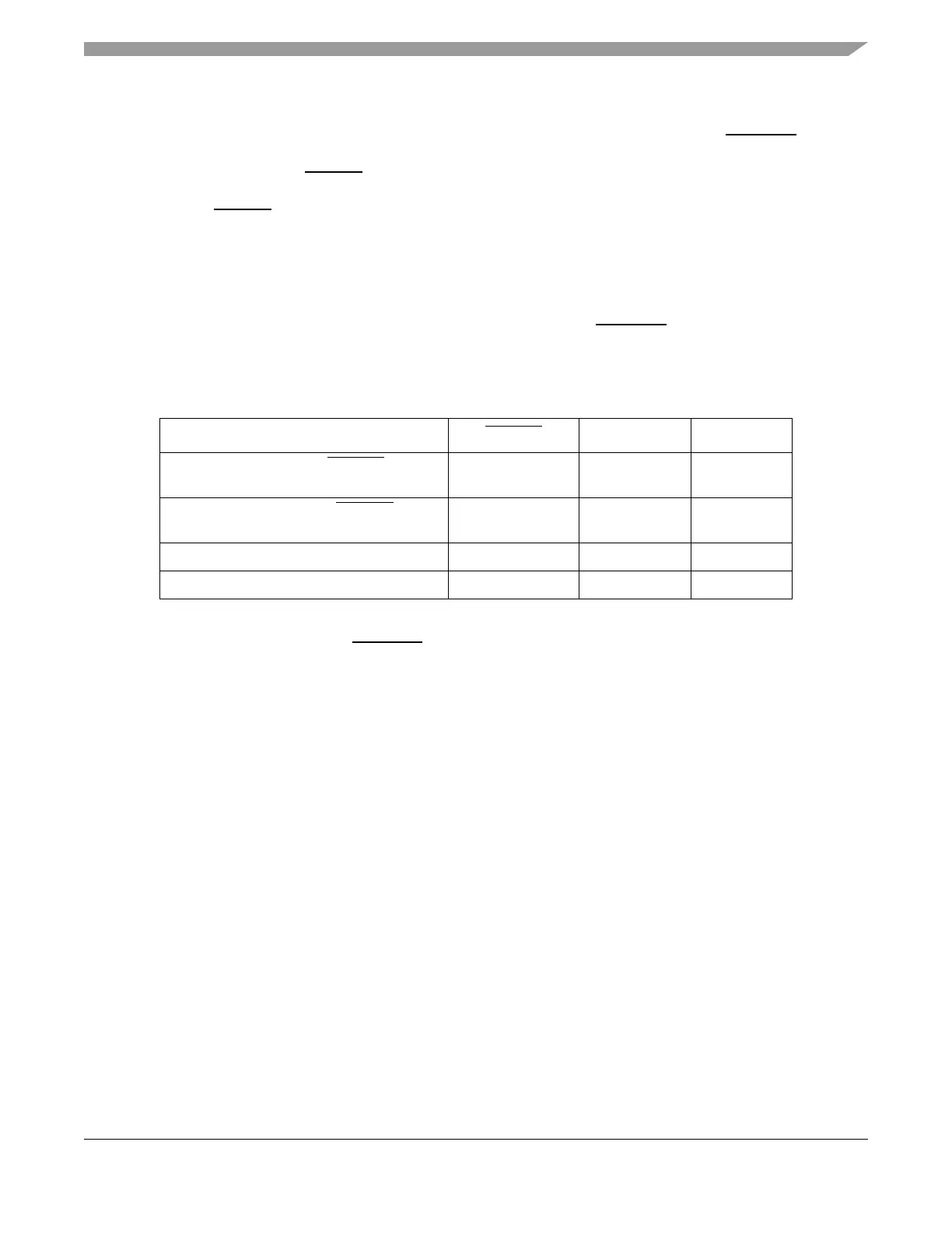
23.5.3.4 Pin Values after Negation of POR
Depending on the final PLL mode required, the PLLCFG[0:1] and RSTCFG pins must have the values
shown in Table 23-2 after POR negates. See application note AN2613, “MPC5554 Minimum Board
Configuration” for one example of the external configuration circuit.
NOTE
After POR negates, RSTCFG and PLLCFG[0:1] can be changed to their
final value, but must avoid switching through the 0, 0, 0 state on these pins.
Table 23-2. Values after POR Negation
Final PLL Mode RSTCFG PLLCFG0 PLLCFG1
Crystal Reference (Using RSTCFG
to select
Crystal Reference as the default)
1——
Crystal Reference (Using RSTCFG to not
select Crystal Reference as the default)
—1—
External Reference 0 1 1
Dual-Controller — 1 —