System Interface Unit (SIU)
MPC5553/MPC5554 Microcontroller Reference Manual, Rev. 5
6-20 Freescale Semiconductor
documentation. For example, for SIU_PCR85 and the pin CNTXB_PCSC[3]_GPIO[85], CNTXB is the
primary function and PCSC[3] is the alternate function. For identification of the source module for primary
and alternate functions, and the description of these signals, see Chapter 2, “Signal Description.” Also see
the chapter of the specific module that uses the signal for an additional signal description.
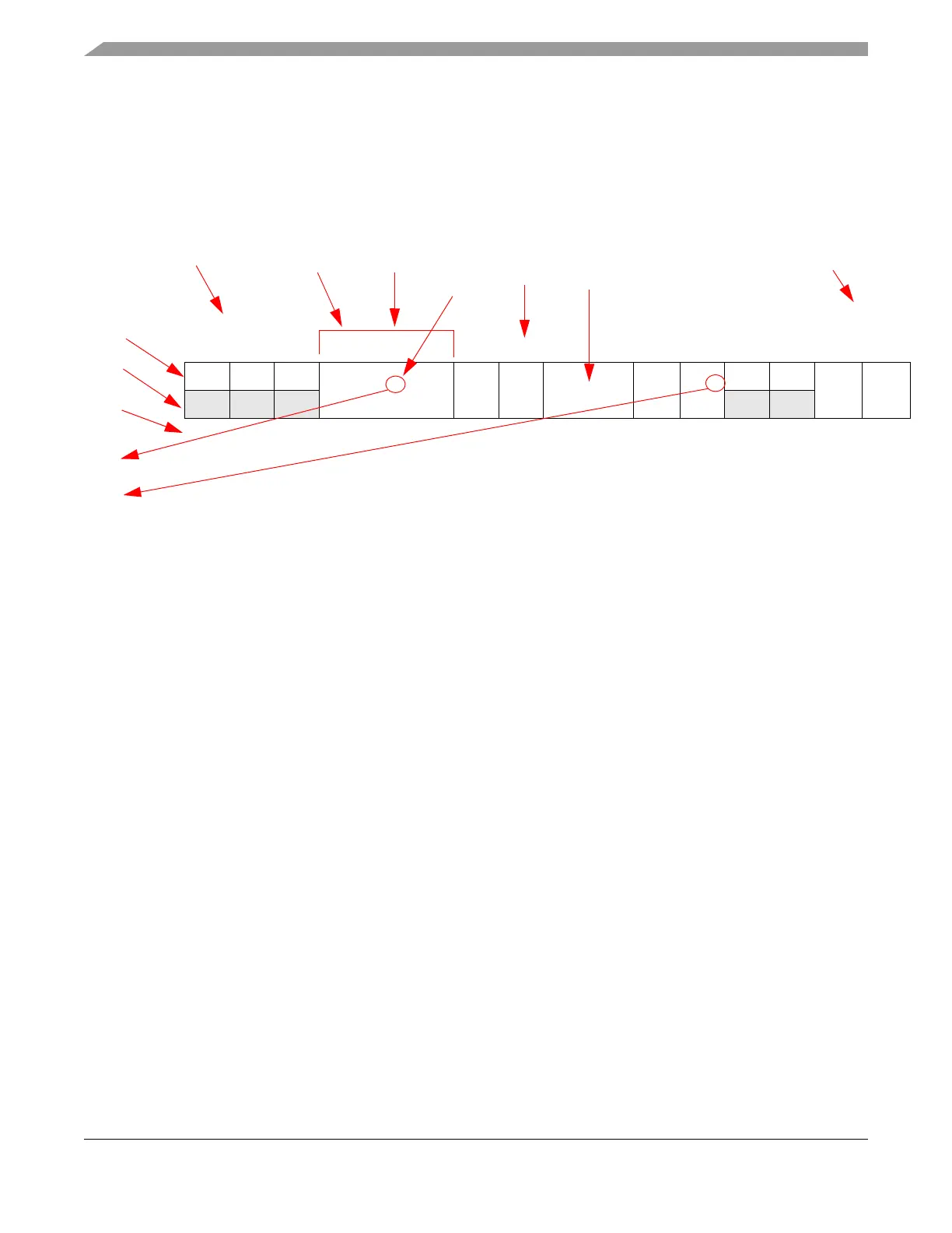
Figure 6-14 shows a sample PCR register with all bit fields displayed:
Figure 6-14. Register Diagram Description
Address: Base + 0x14 Access: Read / write[3:11, 14:15}
0123456789101112131415
R 000
PA
1
1
The PA fields in PCR0 through 3 and PCR4 through 7 must not be configured simultaneously to select ADDR[8:11] as an input.
Only one pin is to be configured to provide the address input.
OBE IBE DSC ODE HYS
2
2
If external master operation is enabled, clear the HYS bit to 0.
00
WPE WPS
W
RESET: 000000001100001 1
Read/write
SIU register address
Read values
Write values
Reset values
access bits
Field
Bit
number
name
Footnotes
Register bit
range [3:5]
Field bit
range [0:2]