MPC5553/MPC5554 Microcontroller Reference Manual, Rev. 5
Freescale Semiconductor 9-25
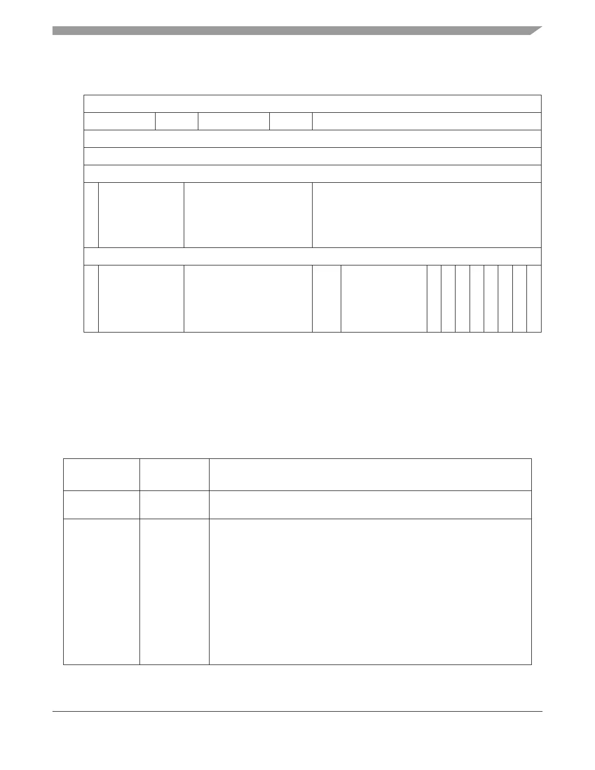
NOTE
The TCD structures for the eDMA channels shown in Figure 9-21 are
implemented in internal SRAM. These structures are not initialized at reset.
Therefore, all channel TCD parameters must be initialized by the
application code before activating that channel.
Word
Offset
012345678910111213141516171819202122232425262728293031
0x0 SADDR
0x4 SMOD SSIZE DMOD DSIZE SOFF
0x8 NBYTES
0xC SLAST
0x10 DADDR
0x14
CITER.E_ LINK
CITER or
CITER.LINKCH
CITER DOFF
0x18 DLAST_SGA
0x1C
BITER.E_ LINK
BITER or
BITER.LINKCH
BITER BWC MAJOR LINKCH
DONE
ACTIVE
MAJOR.E_LINK
E_SG
D_REQ
INT_HALF
INT_MAJ
START
Figure 9-21. TCD Structure
Table 9-18. TCDn Field Descriptions
Bits /
Word Offset [n:n]
Name Description
0–31 /
0x0 [0:31]
SADDR
[0:31]
Source address. Memory address pointing to the source data.
Word 0x0, bits 0–31.
32–36 /
0x4 [0:4]
SMOD
[0:4]
Source address modulo.
0 Source address modulo feature is disabled.
non-0 This value defines a specific address range which is specified to be either the
value after SADDR + SOFF calculation is performed or the original register
value. The setting of this field provides the ability to easily implement a
circular data queue. For data queues requiring power-of-2 “size” bytes, the
queue should start at a 0-modulo-size address and the SMOD field should
be set to the appropriate value for the queue, freezing the desired number of
upper address bits. The value programmed into this field specifies the
number of lower address bits that are allowed to change. For this circular
queue application, the SOFF is typically set to the transfer size to implement
post-increment addressing with the SMOD function constraining the
addresses to a 0-modulo-size range.