MPC5553/MPC5554 Microcontroller Reference Manual, Rev. 5
9-36 Freescale Semiconductor
The exact timing from this point is a function of the response times for the channel’s read and write
accesses. In this case of an slave read and internal SRAM write, the combined data phase time is 4
cycles. For an SRAM read and slave write, it is 5 cycles.
• Cycle n + 1: This cycle represents the data phase of the last destination write.
• Cycle n + 2: The eDMA engine completes the execution of the inner minor loop and prepares to
write back the required TCDn fields into the local memory. The control/status fields at word offset
0x1C in TCDn are read. If the major loop is complete, the MAJOR.E_LINK and E_SG bits are
checked and processed if enabled.
• Cycle n + 3: The appropriate fields in the first part of the TCDn are written back into the local
memory.
• Cycle n + 4: The fields in the second part of the TCDn are written back into the local memory. This
cycle coincides with the next channel arbitration cycle start.
• Cycle n + 5: The next channel to be activated performs the read of the first part of its TCD from
the local memory. This is equivalent to Cycle 4 for the first channel’s service request.
Assuming zero wait states on the system bus, DMA requests can be processed every 9 cycles. Assuming
an average of the access times associated with slave-to-SRAM (4 cycles) and SRAM-to-slave (5 cycles),
DMA requests can be processed every 11.5 cycles (4 + (4+5)/2 + 3). This is the time from Cycle 4 to Cycle
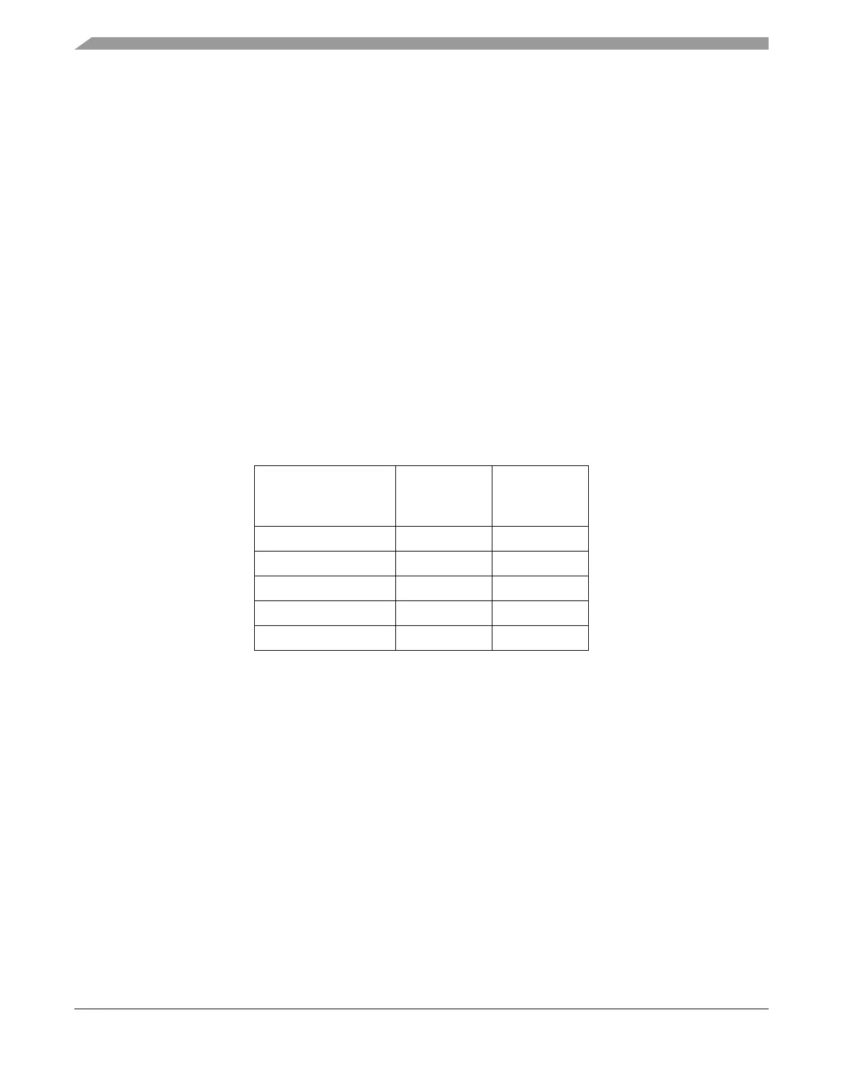
“n + 5.” The resulting peak request rate, as a function of the system frequency, is shown in Table 9-20. This
metric represents millions of requests per second.
A general formula to compute the peak request rate (with overlapping requests) is:
PEAKreq = freq / [ entry + (1 + read_ws) + (1 + write_ws) + exit ]
where:
PEAKreq - peak request rate
freq - system frequency
entry - channel startup (4 cycles)
read_ws - wait states seen during the system bus read data phase
write_ws - wait states seen during the system bus write data phase
exit - channel shutdown (3 cycles)
For example: consider a system with the following characteristics:
• Internal SRAM can be accessed with one wait-state when viewed from the system bus data phase.
• All slave reads require two wait-states, and slave writes three wait-states, again viewed from the
system bus data phase.
Table 9-20. eDMA Peak Request Rate (MReq/Sec)
System Frequency
(MHz)
Request Rate
(Zero Wait
States)
Request Rate
(with Wait
States)
66.6 7.4 5.8
83.3 9.2 7.2
100.0 11.1 8.7
133.3 14.8 11.6
150.0 16.6 13.0